
The hardware implementation
The previous bits of the article ( part 1 and part 2 ) described the core concepts of this measurement and the theory behind it. The actual measurement device - the measurement system is pretty simple when you get right down to it.
What is required and some ramblings
Essentially, all that is needed is:
- a means to switch the nodes between various states - at least two different excitation voltages and a high impedance state
- measurement of voltages on all of the nodes in any state
- send the data to the evaluation system (PC) or evaluation directly on the device
The simplest way of doing the switching and measurements are the GPIO pins of a microcontroller. Most current MCUs have GPIO pins that can be set to either a push-pull mode, in which they are a hard output or into a high impedance input. The microcontroller must obviously have an ADC and the ADC must have a connection to the GPIO pins that connect to the nodes.
There are of course other implementations possible - a crosspoint switch (such as the AD75019 ) would be awesome to use in this measurement, or a bunch of simple muxes, analog/digital switches, or, if you are really into clicky noises, slow measurements, a bunch of relays will serve just as well... the GPIO pins of an MCU are just the cheapest and most convenient method available. Also, an external ADC could certainly improve things. But seeing as the method works well enough with a crappy 10 bit ADC (which is pretty much the lowest resolution ADC in common MCUs these days), it will work better with a better ADC. So it's great for the proof of concept. I am actually working on a device that uses external push pull drivers and an external ADC and should be much more awesome all around, but that's far from ready.
Or, as has been suggested, this could be implemented with multiplexer cards, elite multimeters, or even better SMUs... sadly, I don't have those. If you'd like to donate them (or just donate to me in general by means of money or bitcoins (see donate link on the side) 😉 ) I'll gladly take them of your hands! Really, it'll be no problem!
One of the microcontroller familifes that fit this bill are Atmel Microchip AVRs. I specifically used an ATMega32. Note that that MCU does not do any of the actual calculation - it simply does not have the resources to solve even the small systems of linear equations required for the measurement. There are MCUs that should be powerful enough to do this on their own (certainly some of the mid to high ARM devices).
For a precise measurement, the internal GPIO push-pull driver impedance has to be taken into account. The final output transistors are far from ideal, as such the voltage needs to be measured, not just assumed. It *could* be assumed if the measured setup was of a high enough impedance that the few tens of ohms of the push-pull output stage could be ignored, but it's still better to measure it. If you wish to learn about how/why this is done, check out a few measurements I did to measure the internal resistance of the push-pull drivers on the GPIOs of the ATMega32.
One of the advantages of this kind of measurement is that it does not really care about absolute voltage accuracy - the reference used can be pretty of any value, accuracy etc. provided it stays the same during the measurement of one situation. That's one of the nice things about this measurement - it essentially only takes into account the ratios of the measured voltages, rather than their absolute values. This eliminates the need for a precise ADC voltage reference. Just keep the ADC linear.
The actual device - measurement system
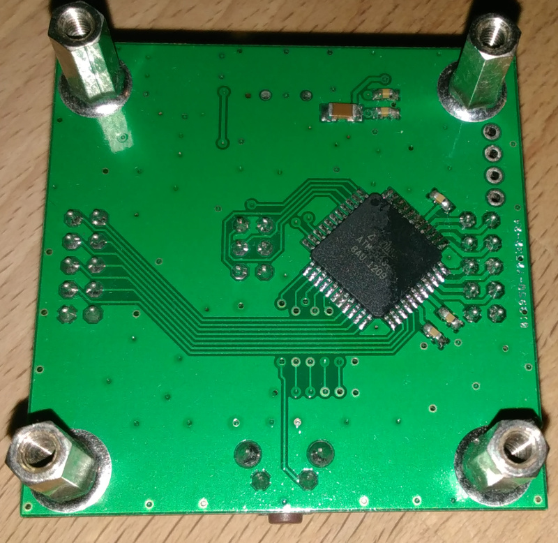
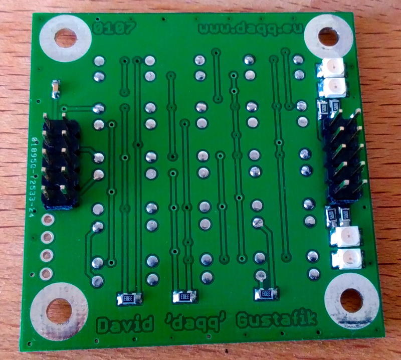
To those expecting some monstrous board with many complex channels - sorry, you will be disappointed. The measurement system is based around an ATMega32 MCU, which communicates with the PC via USB (that is provided via the FT232RL ). The whole system is USB powered, and internally it uses +3.3V as VCC. Aside from the main components there's a little miscellany stuff - power (LF33 LDO, decoupling and misc. filtering), decorational LEDs, a debugging button, an ISP programming connector and the USB connector.
There are two sockets on the board into which the measured board that contains the actual measurement setup. Of these two socket one carries the measurement signals for the nodes ( M_0 - M_7 ), the other one carries some support signals - board identification ( BID_0 - BID_3 ) and some general purpose signals that are used currently to light up LEDs on the measured board ( GP_0 - GP_3 ). That's pretty much it. All of the switching, measurement, muxing is handled by the GPIOs of the MCU, no fancy analog stuff is happening here. The MCU is clocked by the internal RC oscillator, no precise timing is required as far as the measurement is concerned.
VCC is used as one excitation voltage applied to the nodes, the other is GND (0V).
If you want the gerbers or the Eagle source files, you can contact me, and I will send them to you.
Note that the boards were drawn in Eagle. This was before the foul taint of Autodesks monthly ransom bullshit subscription only poisoned Eagle. For future project I will be using Altium Circuit Studio, which I bought for the price of one year of Eagle subscription. So, here are the schematics for the individual bits.
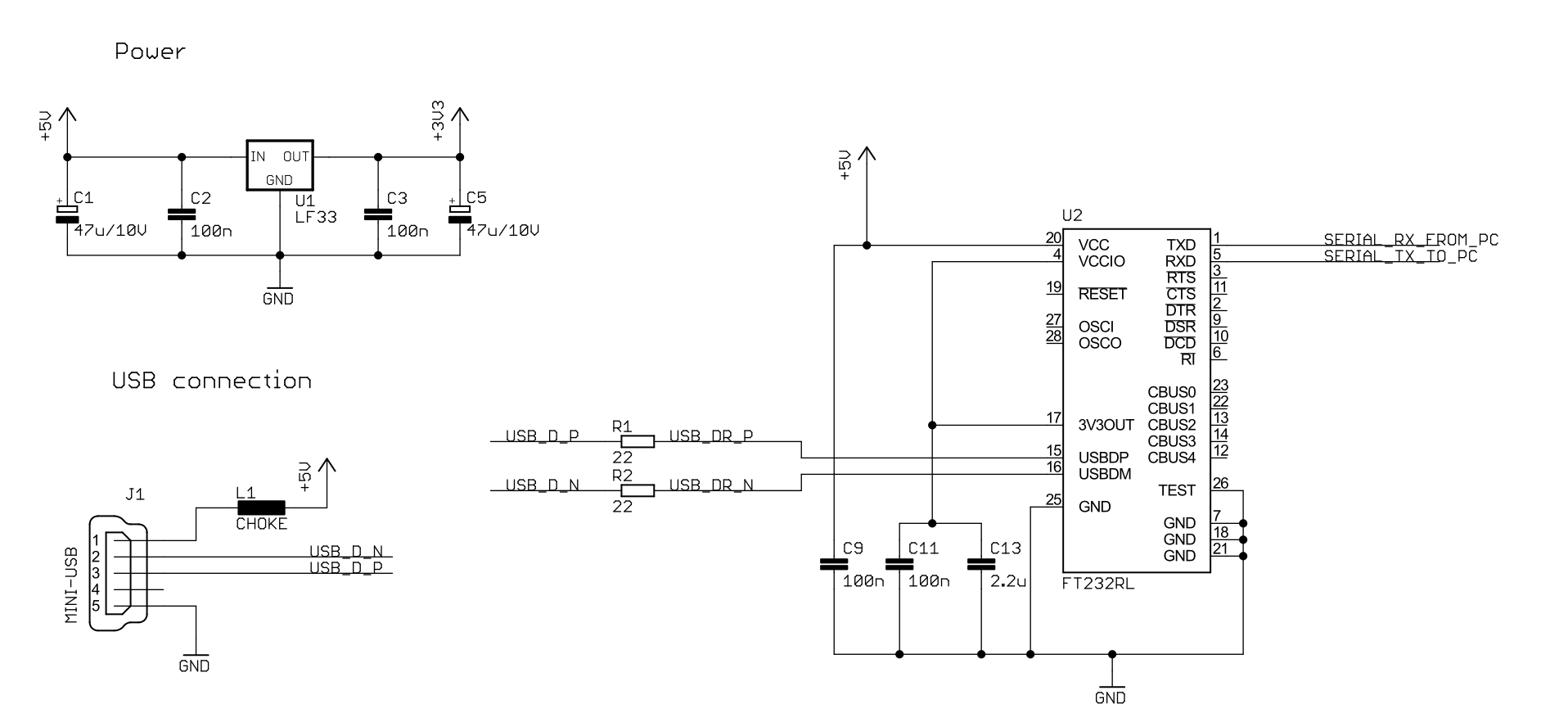
USB and power
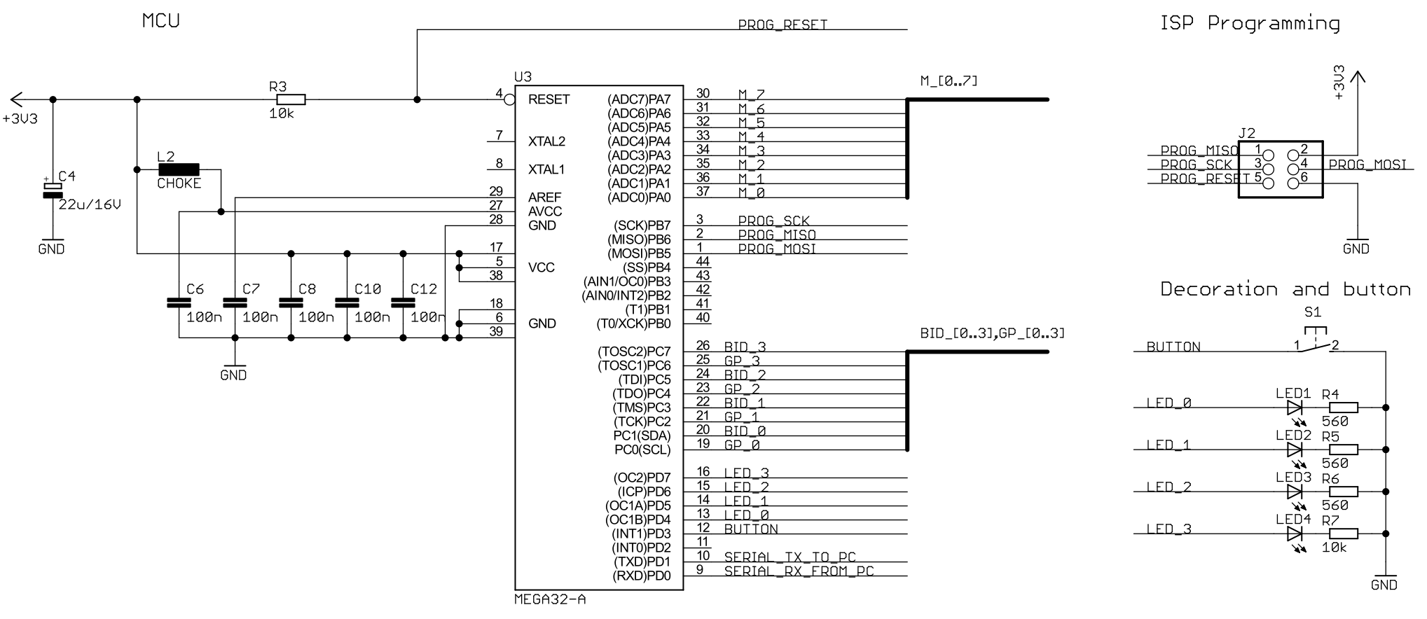
MCU and misc area
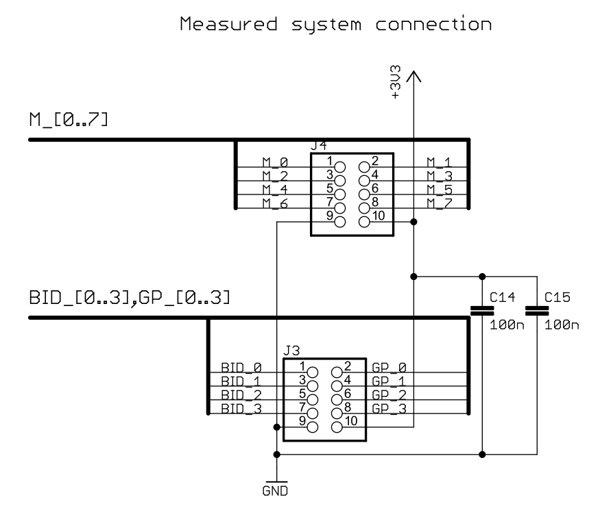
Measured system connection
So, as you can see, nothing special is present here. This could be done with any MCU that meets the before mentioned conditions. All of the magic happens in the software that does the actual math.
And here's the photo of the measurement system. The measured system board can be connected into the sockets, it can be placed nicely above the system.
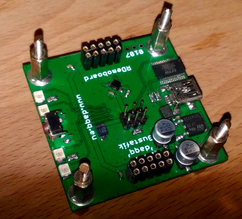
Measurement system top
The bottom side contains the processor and some miscellany parts. Decoupling and such... the connections leading to the measured system, the node ones are done with a thicker and shorter connection. It probably does not make any noteworthy difference, but it's nice and proper.
Measurement system bottom
Mechanically, the boards are of a simple square shape, 50x50mm large. This is my favorite form factor, most notably since having them made costs peanuts and I'm a cheap bastard 🙂 The stand offs are soldered into the board and you can see on the top layer that they are somewhat modified in order to guide the measured board onto the measurement board.
The actual device - measured system board
The measured system can in theory be a horrible mess of cables, or a nicely organized bus. For the purposes of these experiments I made a universal board that can have 28 resistors on it. 25 of these positions can be fitted with both truhole or SMD (0402 to 0805) parts. The schematic for the main part is here:
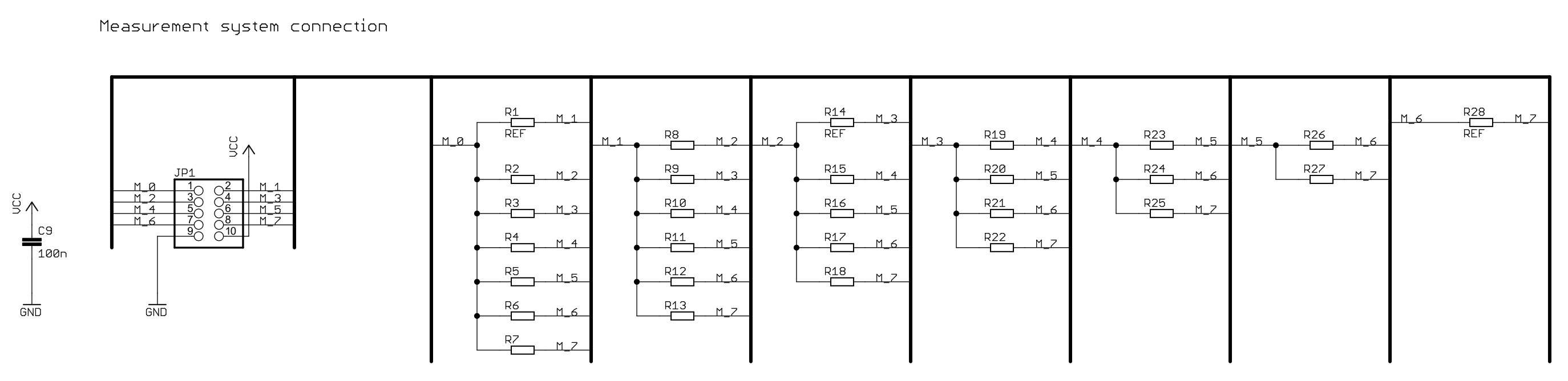
Measured board resistor connections
Click on it for a better resolution. 3 of the positions can only accept SMD resistors and are meant for the reference resistors. These are R1, R14 and R28 as visible on the schematic. These can be either precise known resistors, or individually measured BEFORE they are soldered in. The actual value of the reference resistors should be chosen depending on the value range of the unknown resistors. This will be discussed later, but generally, these should be in the same general area as the unknown resistors. For the 680k thermistors I used 330k reference resistors. For a low impedance measurement I used 300R resistors. The resistors used should be precise and stable. That said, the method can deal with wrong numbers reasonably well.
Again, there is nothing magical on this board - it could just as well be replaced with a lot of wires connecting the individual resistive elements together.
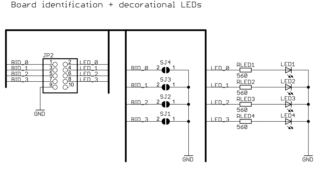
Aside from the main measurement there are two other features on the board - decorational LEDs that are simply meant to light up and indicate activity and a few solder bridge jumpers that can be used to identify the board. A decoupling cap is also present, but not needed - it was added in case I wanted to hack something onto the board and it needed power. The schematic for the miscellany part of the board is here:
Miscellany connections
The important signals on the board are the individual node signals ( M_0 to M_7 ), that connect all of the resistors. Aside from that there are the LED signals ( LED_0 to LED_3 ) and the board identification signals ( BID_0 to BID_3 ).
The following is a table showing the connection of the individual resistors with the nodes:
| Name | Node A | Node B | Note |
|---|---|---|---|
| R1 | 0 | 1 | Reference |
| R2 | 0 | 2 | - |
| R3 | 0 | 3 | - |
| R4 | 0 | 4 | - |
| R5 | 0 | 5 | - |
| R6 | 0 | 6 | - |
| R7 | 0 | 7 | - |
| R8 | 1 | 2 | - |
| R9 | 1 | 3 | - |
| R10 | 1 | 4 | - |
| R11 | 1 | 5 | - |
| R12 | 1 | 6 | - |
| R13 | 1 | 7 | - |
| R14 | 2 | 3 | Reference |
| R15 | 2 | 4 | - |
| R16 | 2 | 5 | - |
| R17 | 2 | 6 | - |
| R18 | 2 | 7 | - |
| R19 | 3 | 4 | - |
| R20 | 3 | 5 | - |
| R21 | 3 | 6 | - |
| R22 | 3 | 7 | - |
| R23 | 4 | 5 | - |
| R24 | 4 | 6 | - |
| R25 | 4 | 7 | - |
| R26 | 5 | 6 | - |
| R27 | 5 | 7 | - |
| R28 | 6 | 7 | Reference |
The placement of the reference resistors may seem arbitrary, but if you take a closer look you will note that they do not share any nodes. This should improve the results slightly by distributing the knowns closer to the unknowns and "connecting" them more closely. It makes sense from a mathematical point of view 🙂
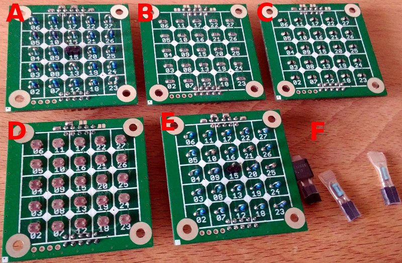
Here are some photos of measurement boards - they are of the same basic design, only with different parts placed.
Measured board top side photos
These boards contain the experiments I did. They are populated as follows:
- A - high impedance test board with connector on R15
- B - high impedance test board
- C - thermistor board populated with 680k @25 °C resistors
- D - photoresistor board
- E - low impedance test board with connector on R15
- F - 51k, 10k and 100R resistors that can be fitted into the connector on the test boards
The bottom side contains the reference resistors and the connectors that connect up to the measurement system. Also, there are decorational LEDs, because blinking is fun!
Measured board - bottom
Again, mechanically the board is a 50x50mm square, that fits atop of the measurement system.
Firmware
I will be discussing the firmware later on. It's nothing magical, just a few hundred lines of C. Not Arduino mind you.
Conclusion - hardware, firmware
So, that's that. As you can see the hardware needed is pretty trivial and the method can be implemented using a cheap off the shelf MCU. Obviously, if you would use better parts, faster, higher resolution ADCs, professional DAQ systems, you'd get better results.
But the point of this minimalist hardware demonstration was to show that nothing particularly exotic is needed and that the magic lies in the math and the software rather than the hardware.
So, that's that! Stay tuned for part 4, where I'll be discussing the software... which is an unholy mess that will send any proper .NET programmer running, shrieking in horror and revulsion. Sorry.