The HP 3476B multimeter is a neat piece of measurement equipment - probably one of the better choices for an economical (sold at 225 USD in 1976, around 1k USD today) 3½ digit digital meter in the later 1970s. It can measure DC and AC (45Hz to 5kHz) current and voltage as well as resistance. There were two versions made - the A version and the B. The only difference as far as I know was that the B had internal NiCd batteries and as such could be carried around. It also had an internal charger that took care of the batteries. This was given to me by a very good professor on my old high school - I have fond memories of him and the school.
To download the service manual, click below:
[wpdm_file id=21]
Warning, it's a 13 MB file... but it's interesting reading.
NOTE:
No electronics were harmed during this teardown. Precautions were taken to avoid ESD and the other popular ways to kill stuff. After reassembly the meter is working just as well as it did before.
The Big Picture
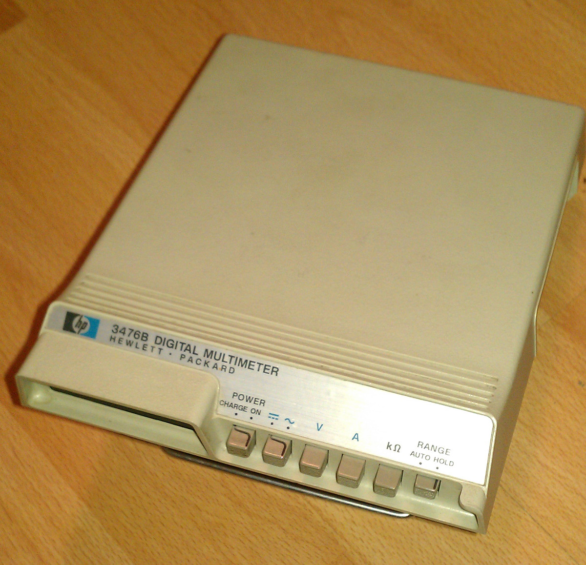
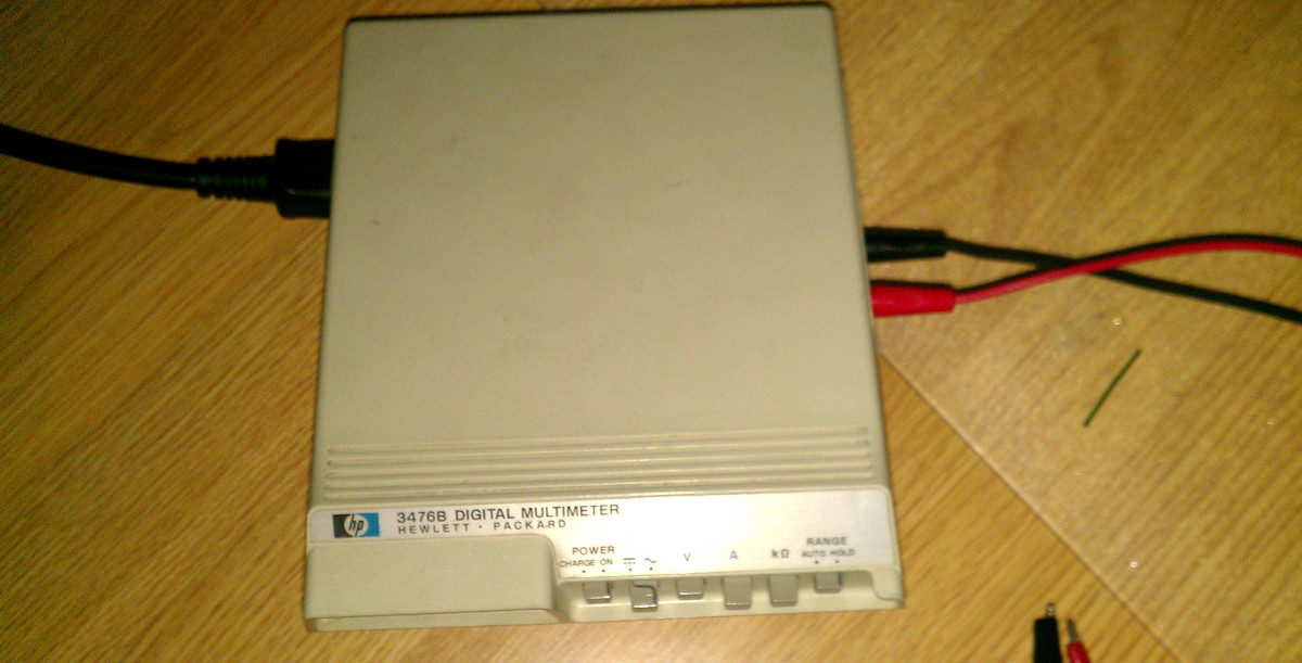
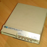
Here's a top view of the device:
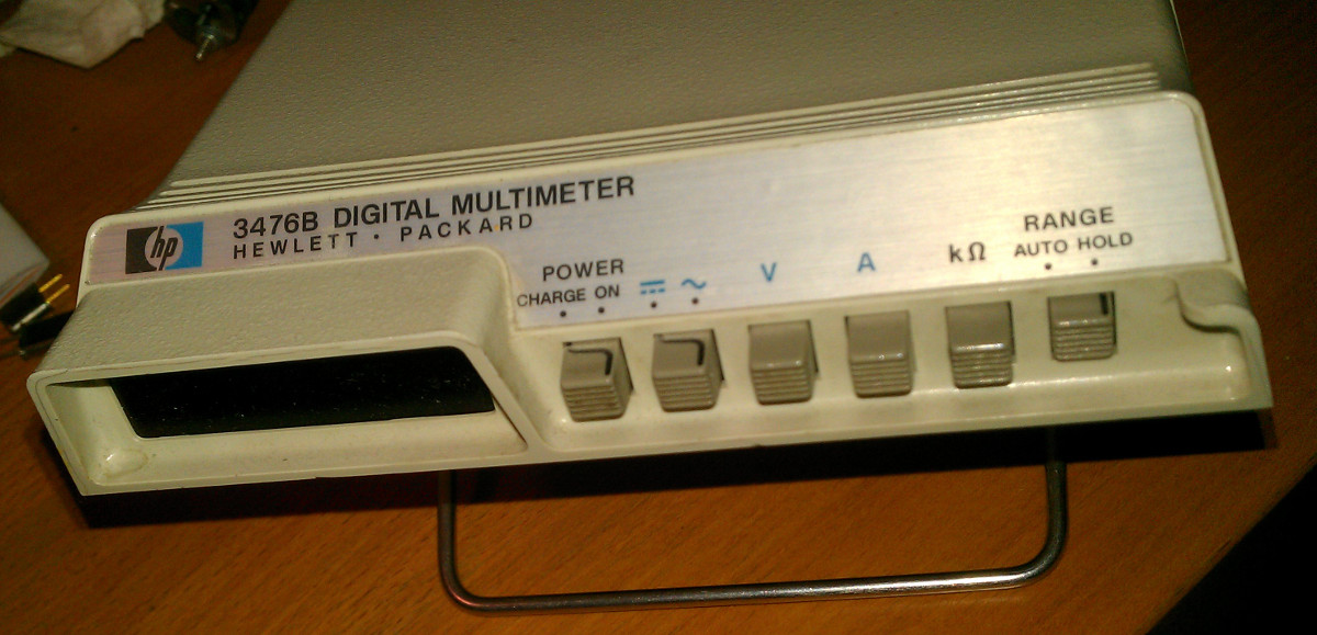
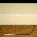
It's a bench top or portable unit - it's pretty compact and the design is very straight forward. It is an autoranging multimeter, with optional range hold. I really like the design. A front view:
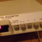
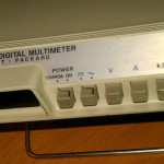
Nice buttons, clearly visible functions. It has an LED display - a standard for the era. Its readability is good, only the digits could be a bit bigger:
It's the same type of display that was used for the calculators of the era. But I guess it was a good choice at the time given the size, layout and battery life considerations. It's not meant to be viewed from a too wide angle.
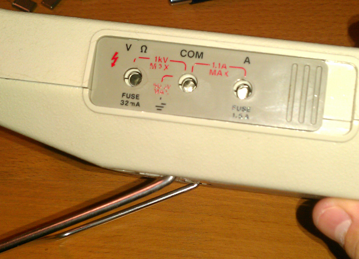
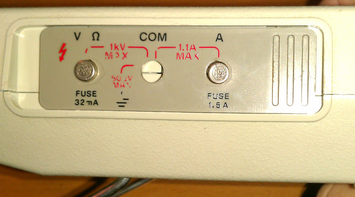
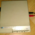
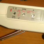
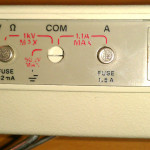
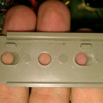
The probes were inserted in from the side of the device - another neat feature - when you slide the gray plate to the side the fuses pop out and can be changed.
Now this is my only objection to the design - you need to connect something from both sides to make it work - ads a lot to the space requirements.
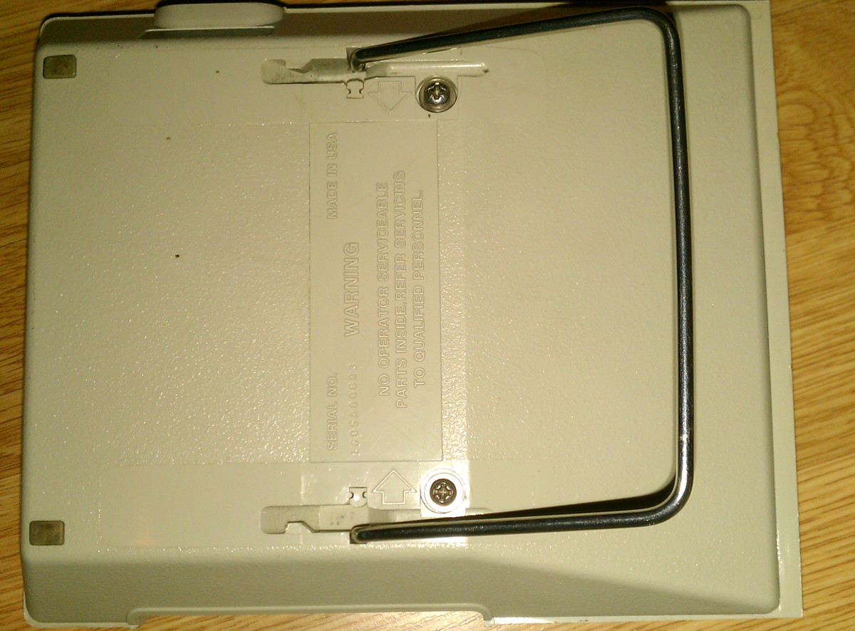
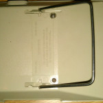
The bottom of the meter is where the screws and the standoff is located:
As there are no user serviceable parts inside we'll just leave it alone and... Naaaah... We'll open the bugger.
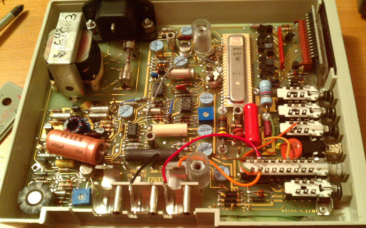
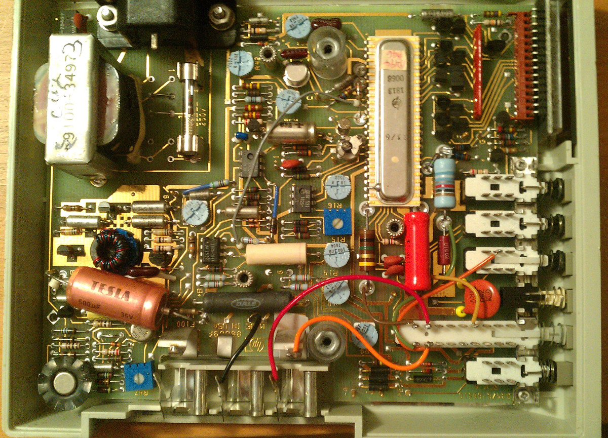
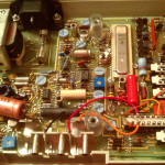
All of the electronics are on one board that occupies the whole inside. It's a two sided, heavily gilded all through hole technology board. There's a few jumpers and connection cables flying around the board. Now for the various parts.
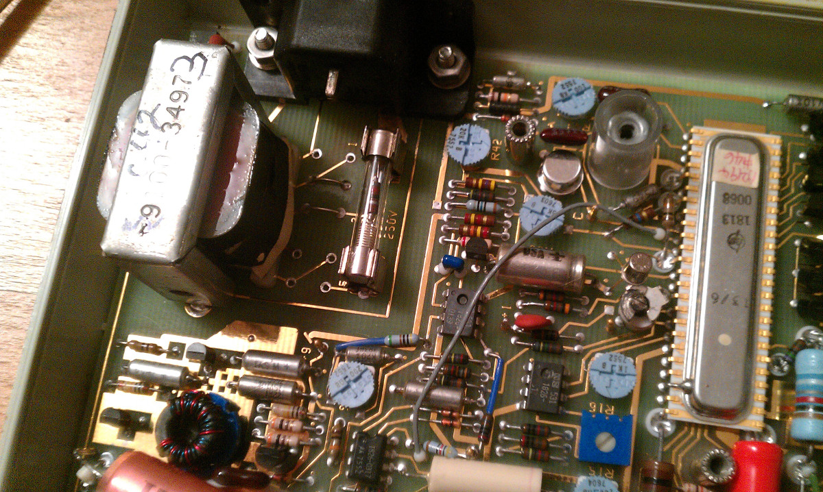
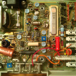
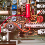
The power supply is a mains transformer with jumpers that set what voltage is used. The transformer has multiple windings, can accept from ~86V to ~230V AC based on the jumper settings - a neat and cheap way to do it. The fuse is interesting - a resistor or some such is in series with the actual fuse. The whole system is floating relative to the mains ground, only the transformer body is grounded. The main rectifier is behind the transformer.
The actual voltages are generated by a linear stabilizer and a DC DC converter. See the manual for more info on this - it's interesting reading.
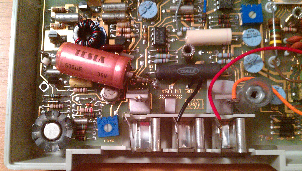
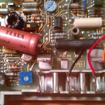
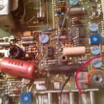
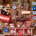
Next up is the charger circuit region - you've probably noticed the out of place Tesla capacitor. Tesla was a Czechoslovakian state owned electronics megacompany. So, were their products so amazing that HP needed them in their products? Nope, it's just a silly replacement of the NiCd batteries. I didn't do this hack, who am I to judge?
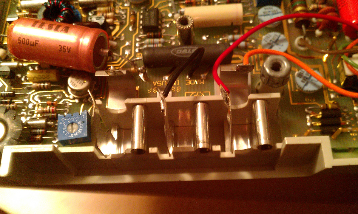
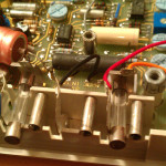
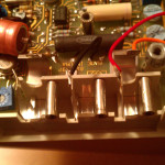
This here is the probe input connector - when interacting mechanically with the gray plastic cover this serves a dual purpose - a connector for the probes as well as a holder and connection for the fuses. Also it ensures that whilst changing the fuses no probes can be connected to the inputs. This is far better than the current state of things where you have to disassemble your whole device to change a fuse or battery.
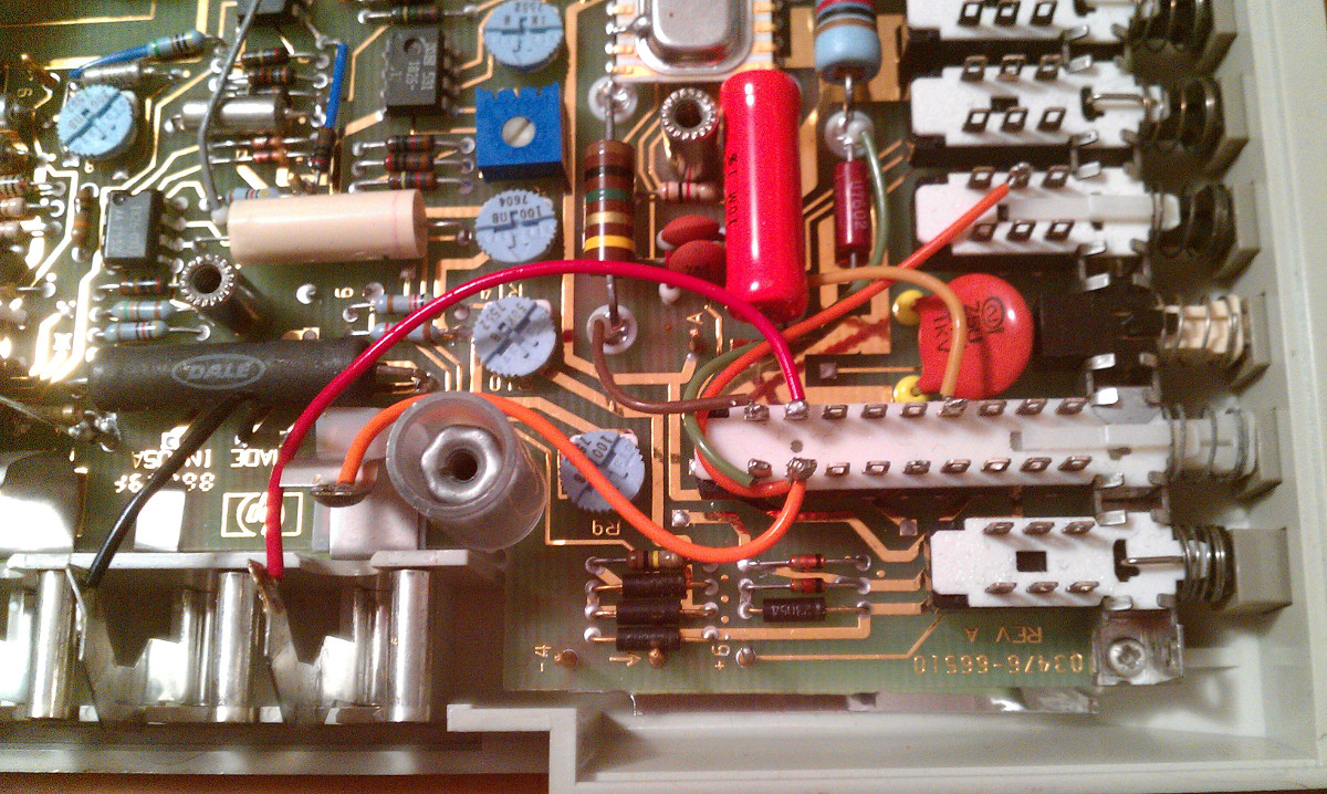
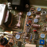
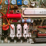
The inputs are connected directly to the function selection and power enable switches. Note the current sense resistor right behind the input terminals. There is some input protection and biasing - see the manual for more detailed info on this.
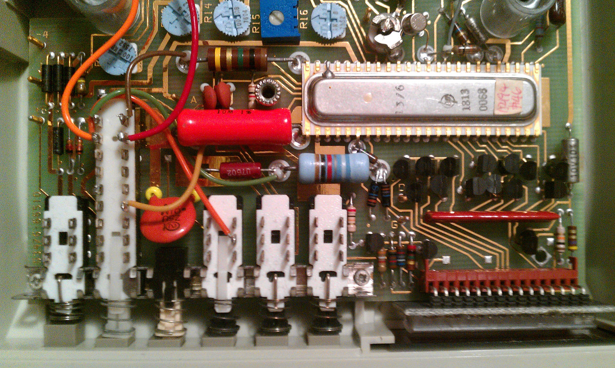
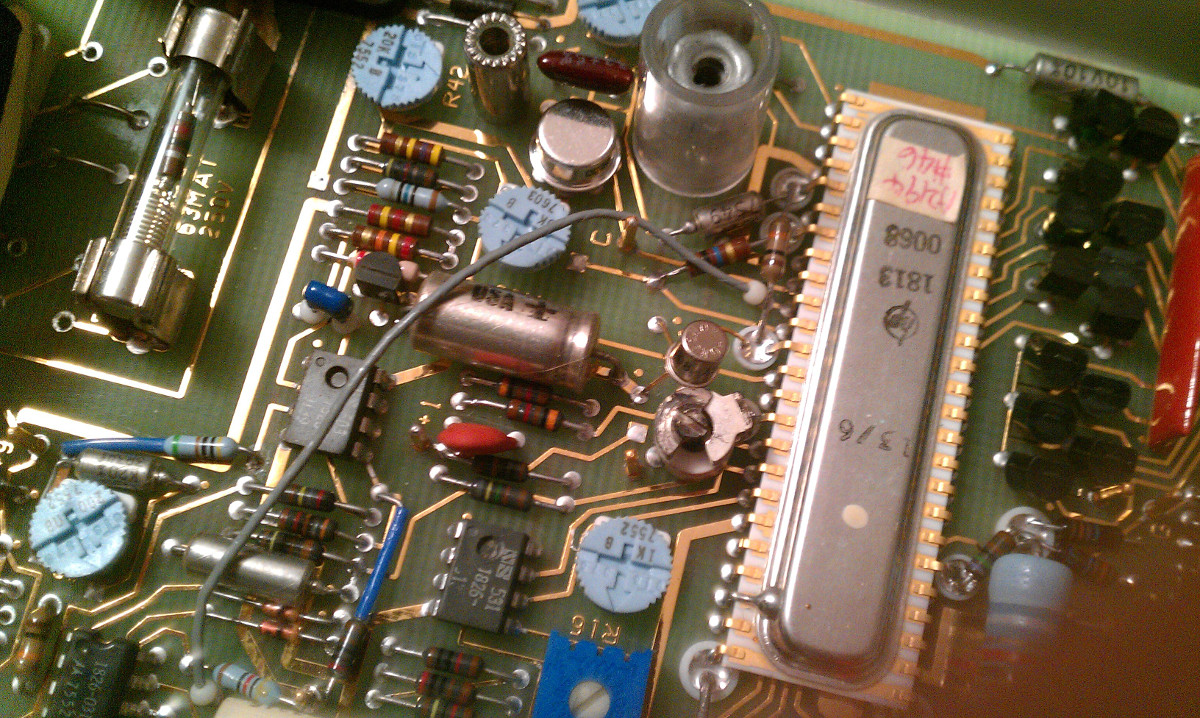
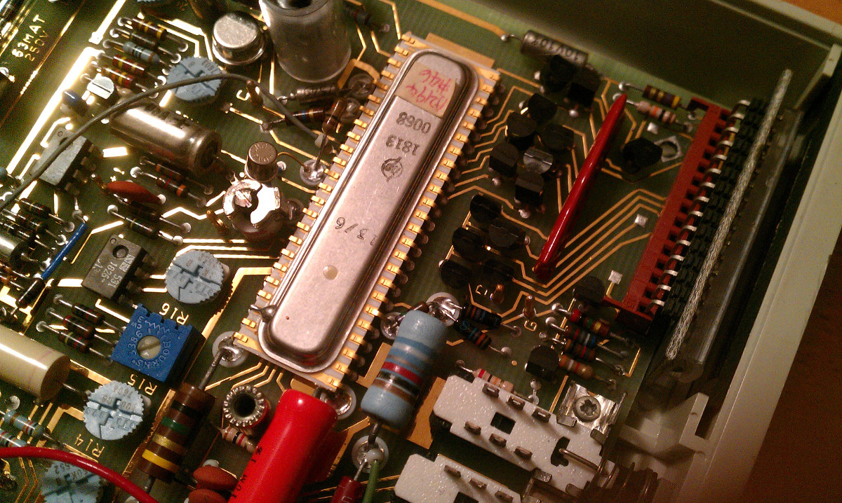
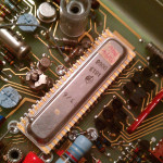
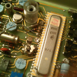
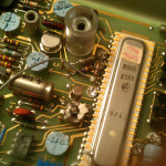
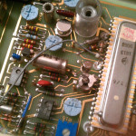
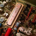
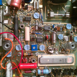
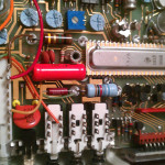
The input switches also provide logic signals for the main ASIC to know what we want of it. Now onto the ASIC - most of the actual function, conversion, logic and black magic is done here. Note the crazy package. The ASIC is most likely a hybrid device with multiple ICs and discrete components as well on a single ceramic board. It contains some of the reference resistors/dividers, switching, conversion and display logic... pretty much everything aside from the AC converter and the main integrator, which is located outside of the IC in discrete form made out of an op amp and some discrete parts. So no single part ADC...
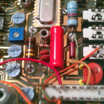
There's a lot of trim pots all around the place.
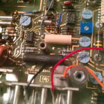
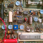
Even with an economical option HP took the safe path and for those really high impedance traces included teflon standoffs as you can see above - this had to be horrible to solder - I wonder if they first wave soldered the bulk of the parts and later hand soldered the specialties or in reverse. Note several pin of the man legged monster that do not connect to the board but rather go directly into a standoff. Must have been a hell of a thing to assemble.
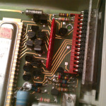
The transistors that drive the LED display are directly connected to the ASIC. The display is a 5 digit device being run in a muxed way at a frequency of around 800Hz (depending on the line frequency, which is interesting...)
There's a lot of things that need adjustment - this small board contains 11 (!) trimpots, a fair amount of test points.
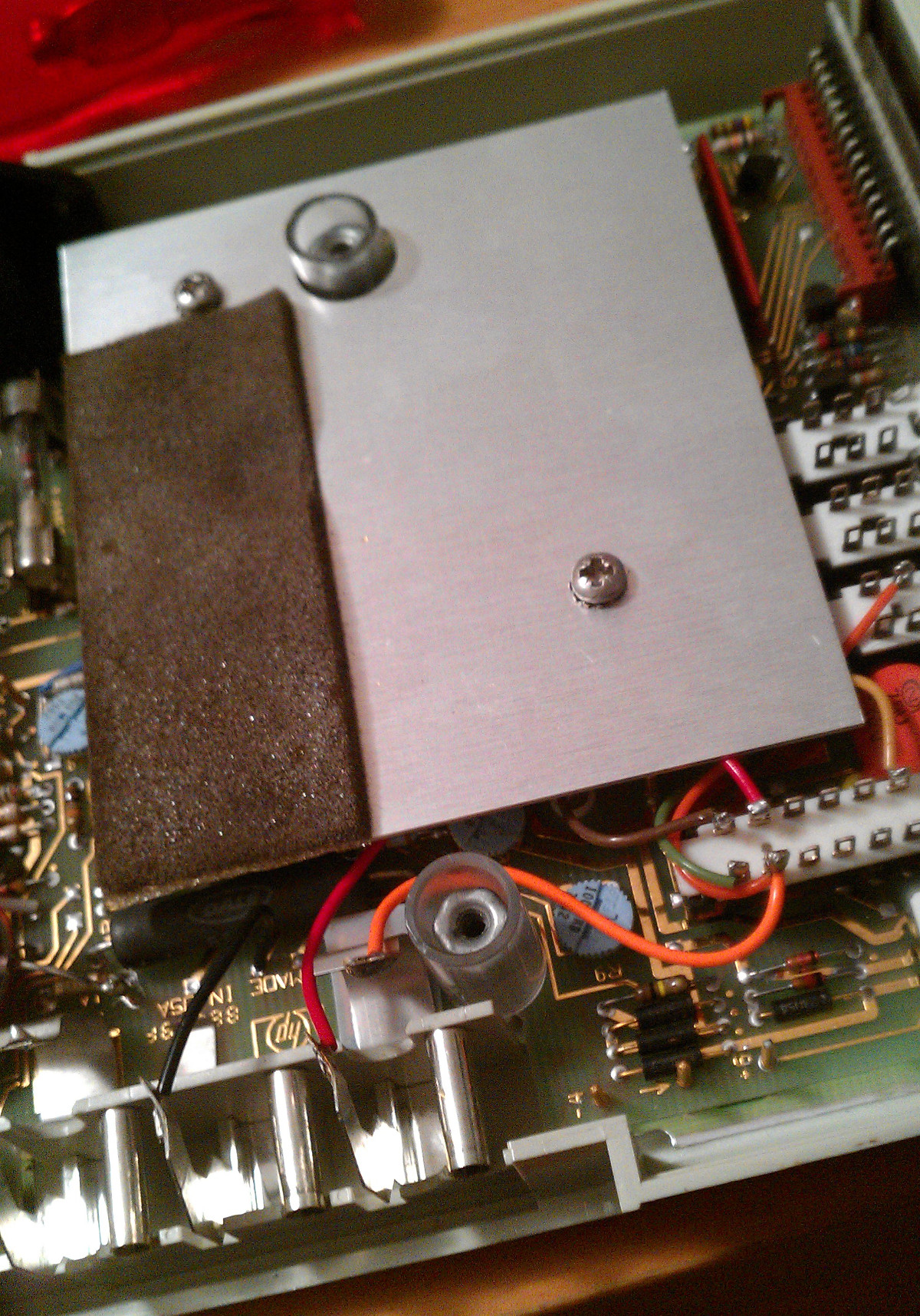
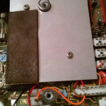
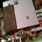
And that's about it. There's a shield above the main system:
It's probably also the place where the battery pack went before it died.
Conclusion:
This is a nice meter. Some things I do object to - the not exactly wide view angle of the display, the fact that you need to connect things to both sides to make it work, but other than that it's a fine unit. I would also want to thank my professor for this device. Hope you enjoyed this, share if you did 🙂
- Display readability
- The main body of the HP 3476B DMM
- Meter in use
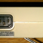
- The main plug
- The bottom
- Behold – the Backside
- Side panel
- The front panel
- Fuses popped out
- Display being used
- Shield? Yup, here.
- Input jacks assembly
- Main ASIC and surrounding area
- Teflon standoffs detail
- Power supply area
- Trimpots! Trimpots everywhere!
- Input switches, display and ASIC
- Input connection to the function switches
- The megabatterycapacitor!
- The big picture



3 Responses to HP 3476B teardown