
The HP 6010A is a monster of a power supply, capable of providing 1kW. There are three limits: 17A, 200V and 1kW - that means that you can source 200V, but only up to 5A. You can suck 17A, but only at up to 60V.
I got this one second hand, possibly third or eight hand. Some butchery has been done - some parts were replaced (the old ones probably blew).
All in all, the device is a big power supply, not meant for precision but rather for power. The power supply works well, though I've yet to test the 1kW - it's not exactly easy to sink 1kW of heat 🙂
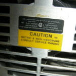
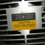
To download the service manual, click below:
[wpdm_file id=22]
It's really good reading... well, more like looking at schematics and thinking that the good people at HP... or is it Agilent? No, wait! It's Keysight Technologies! I'm sure they had a good reason for renaming it... again... probably something involving illegal herbage and marketing. Anyway, the good people there were a really smart bunch apparently.
NOTE:
No electronics were harmed during this teardown. Precautions were taken to avoid ESD and the other popular ways to kill stuff. After reassembly the power supply is working just as well as it did before. Though it does kind of scare me...
The Big Picture
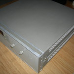
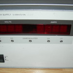
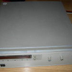
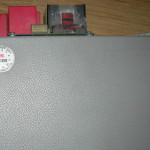
This power supply's design is strictly functional. It can be described as a gray box with meters in the front.
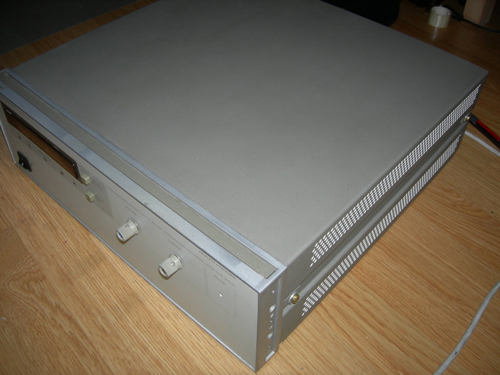
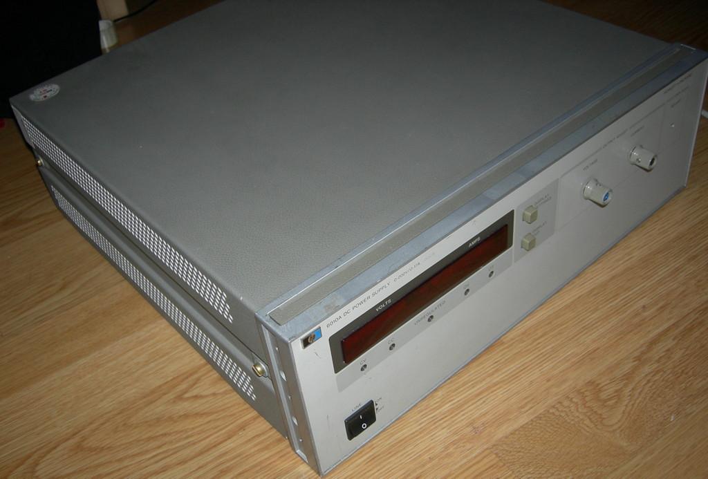
The whole device
It's a weighty beast - a little over 20 kg. Should be packed with goodies! Now, let's look at the box more closely.
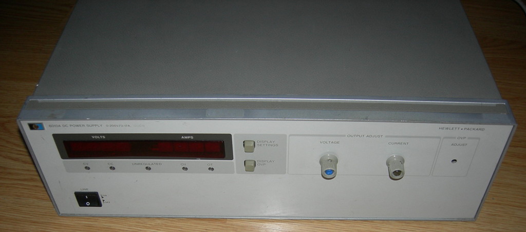
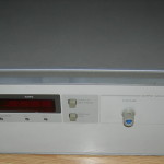
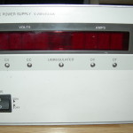
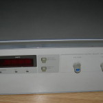
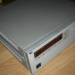
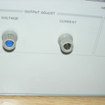
The front panel
The front panel is exactly what you'd expect - a nice clean layout, you can set your current and voltage values, choose what you're displaying - whether the current value, or the value you've set. You can adjust the overvoltage protection as well. And that's about it. Some little indication is provided to tell you whether you are running in a constant current or constant voltage mode. Oh, and there's a power button. The bastard doesn't have output jacks (well, at 17A it's more along the lines of rails) on the front! That's it for the front panel.
Side view
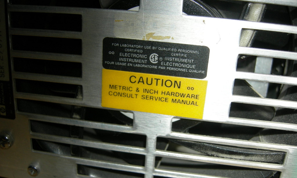
The side of the device is not interesting at all. To enable airflow, both of the sides have a grid of holes. The main chassis is held in place by four really big screws on the sides.
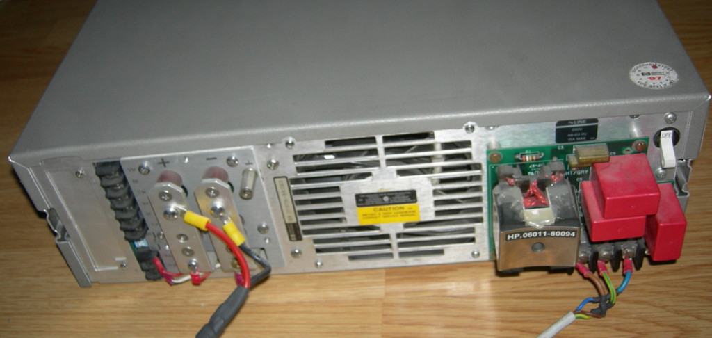
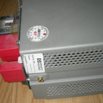
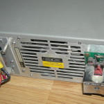
The backside
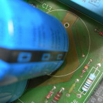
The backside is where a lot of the magic happens - here is where you plug the power, get the output, get external signals and put a lot of air. First of you'll notice that there's no power connector as such, but rather a board with a gargantuan mains filter, because GO TO HELL EASE OF CONNECTION, THAT'S WHY!
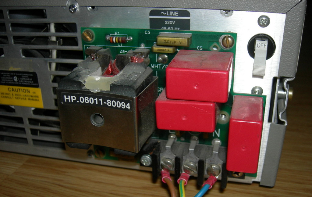
Mains filter
I'm sure that an adjustable switched 1kW power supply does need a lot of filtering to avoid crappin' up the mains city wide, but come on! Couldn't you just have added at least a power connector? Normally this whole area is covered by a plastic box and a mains cable goes out of it. Mine didn't have the box, but had a lot of glue. The filter buzzes slightly even when turned off. Oh, and there's a main power switch/circuit breaker. I don't like this part at all. I'm sure they had their reasons, but I don't like it.
Fffffffuuuuuuu......
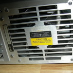
The fan is as boring as it gets, until you read the sign, when you get a sense of dread... USING TWO UNIT SYSTEMS, ONE OF THEM IMPERIAL??? WHAT'S WRONG WITH YOU?

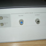
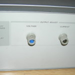
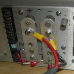
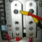
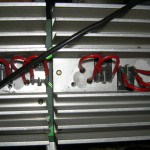
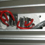
Output rails
The third part of the back side is interesting - at 17 Amps you can't just use regular banana jacks... well, you can use some special ones, but... It's probably simpler to just use a big aluminum rail and be done with it. Let the user screw whatever he wants there. M4 screws are used for the connection. There are several output/inputs for the device. It does allow a little remote usage/control, but analog only. There's a slot for an optional card/block there as well. The 6010A was one of a family.
And that's about all we'll learn from the outside. The bottom is really boring. So, let's get in!
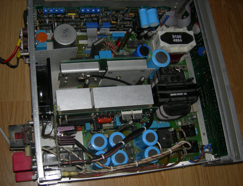
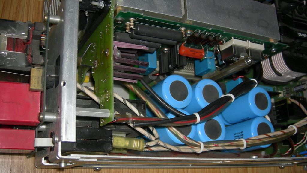
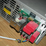
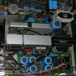
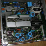
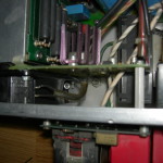
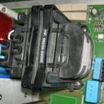
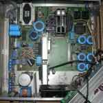
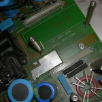
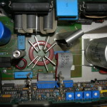
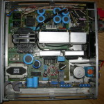
Behold, the Kraken!
After taking the lit of, the first thing you'll notice is the really big versions off parts that are normally (at least in my world) smaller. Really big switched transformers, really big caps, really big somethings. And big ass resistors.
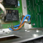
Mains input board connection
The mains input/filter board is connected to the inside using three big wires. The mains wire is connected through a circuit breaker, into the main board.
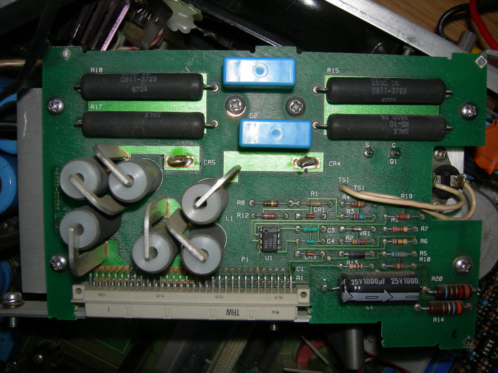
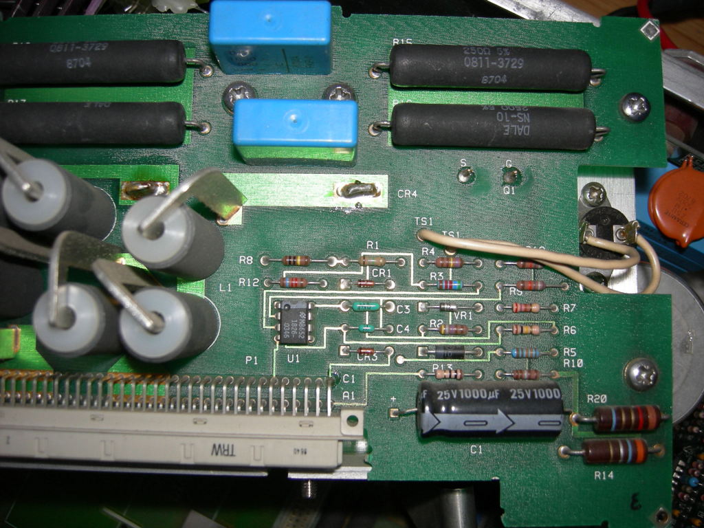
Power path
Mains landing
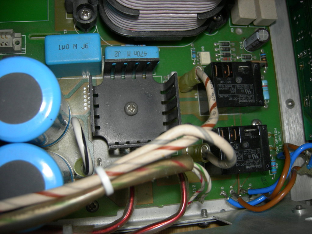
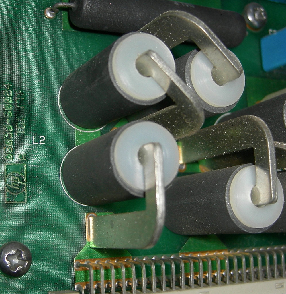
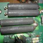
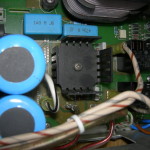
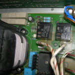
The mains are then split into two - one part goes of to a transformer that does the support stuff - powers the analog and control stuff. It's switched by the front panel switch. The second part of mains goes into a soft start circuit with these beastly relays. After that it is rectified and filtered rather seriously. There are bleeder and balancing resistors all over the place.
Bleeders, filters, the lot...
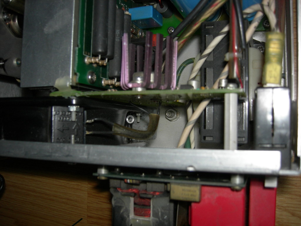
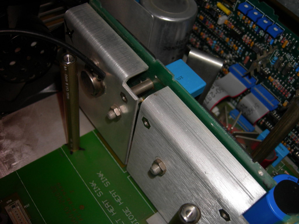
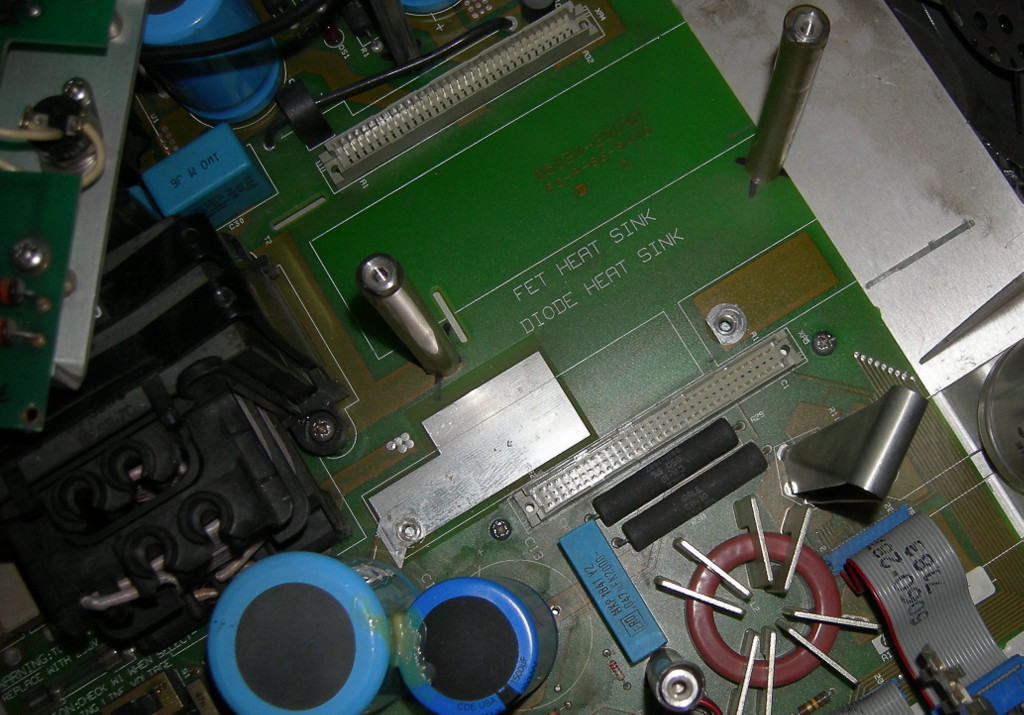
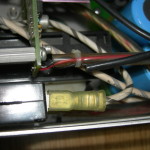
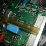
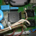
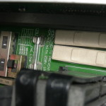
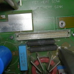
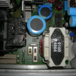
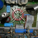
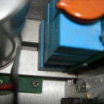
The actual switching is done on outside of the main board on a socketed board on a DIN connector. This was most likely done to get more actual physical space as well as enable more efficient cooling - the FET board is perpendicular to the main board.

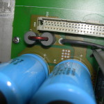
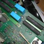
FET board connector
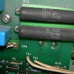
There's nothing interesting on this part of the board. However, leading directly into it you can see T1 - a current transformer that provides some of the black magic feedback that drives this puppy.
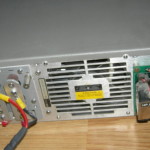
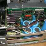
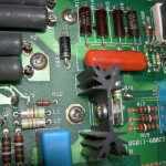
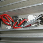
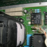
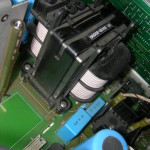
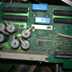
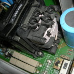
FET board top
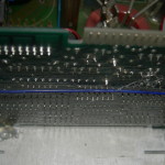
The FET board does all of the switching as well as the control and protection of the FETs, the feeding of the tranformer, some filtering... A lot of the magic happens right here. The transistors get their signal from somewhere else, but they are at the heart of this device. See the manual for details.
Note the little transformers on the board at the top - they are how the transistors are power isolated from the control part. Now, this is one scary setup switching setup. On the right part of the board is the driver part. Well, most of it.
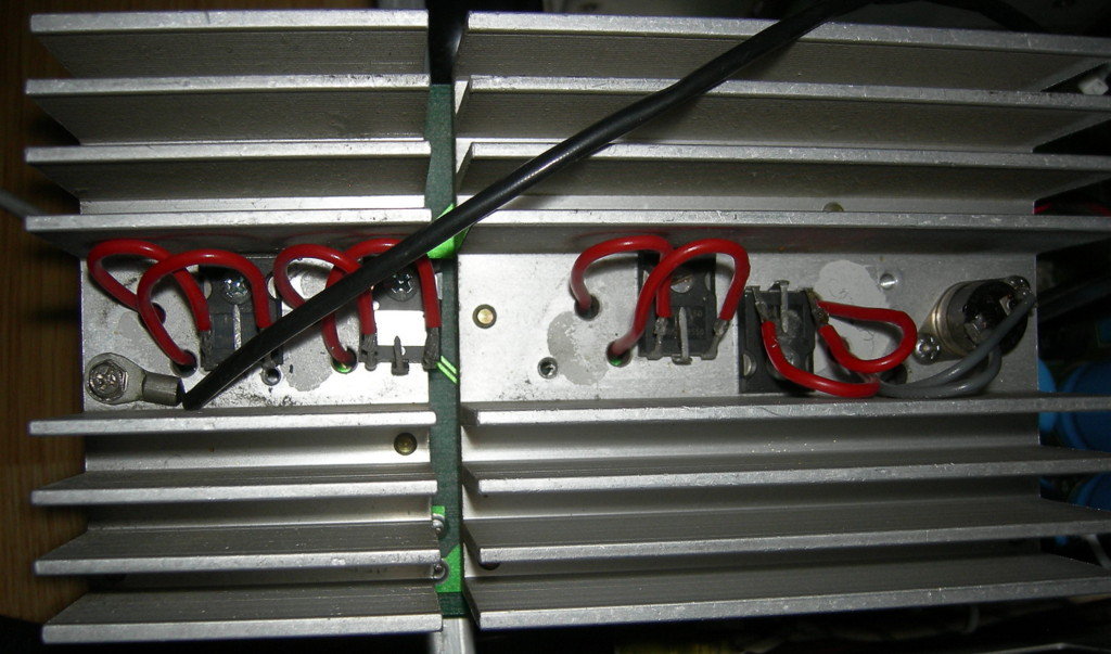
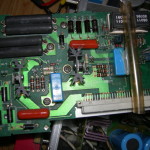
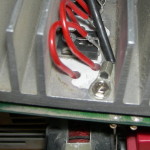
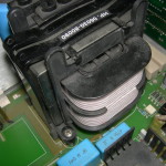
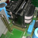
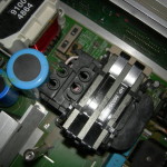
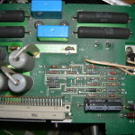
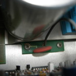
FET board top - butchery
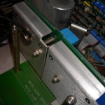
Remember when I mentioned that this had been serviced? Well, here is one part of the servicing. Somewhat butcherous, but it works apparently. Poor FETs. Note the heatswitch on the heatsink - it's supposed to trigger at 95 deg.C. From the second heatsink a temperature probe is lead.
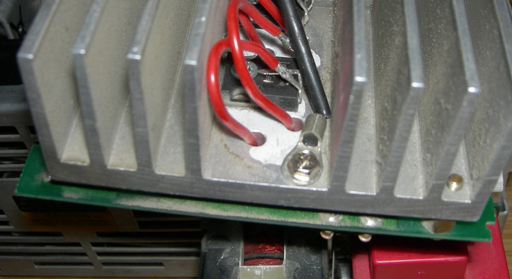
Well, it works...
The FETs are there to feed the giant transformer. Here we have it:
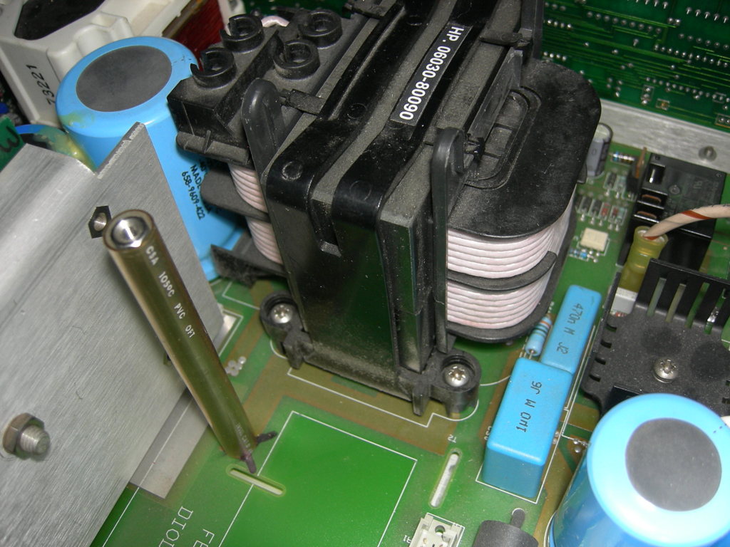
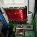
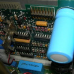
Hey there, big fella...
It's really big for a switched transformer. And the windings are really huge.
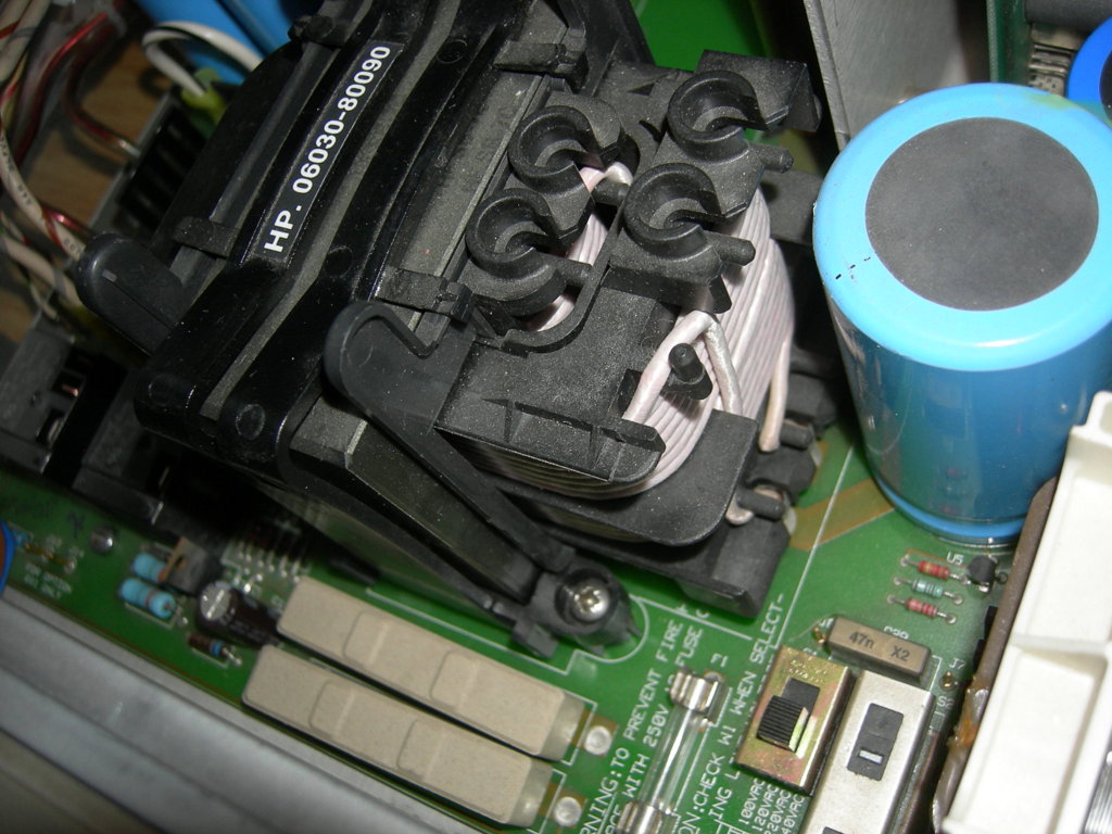
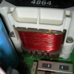
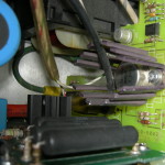
Behind the transformer
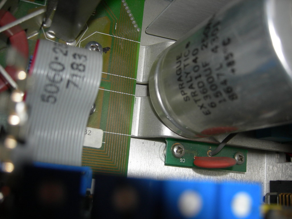
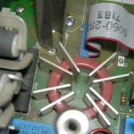
The transformer is a simple one - two windings only - the input and the output. From the transformer it's onto the rectifier board. The rectifier is also housed on a separate board - the diode board.
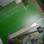
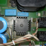
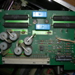
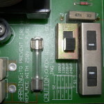
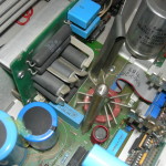
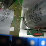
Diode board top
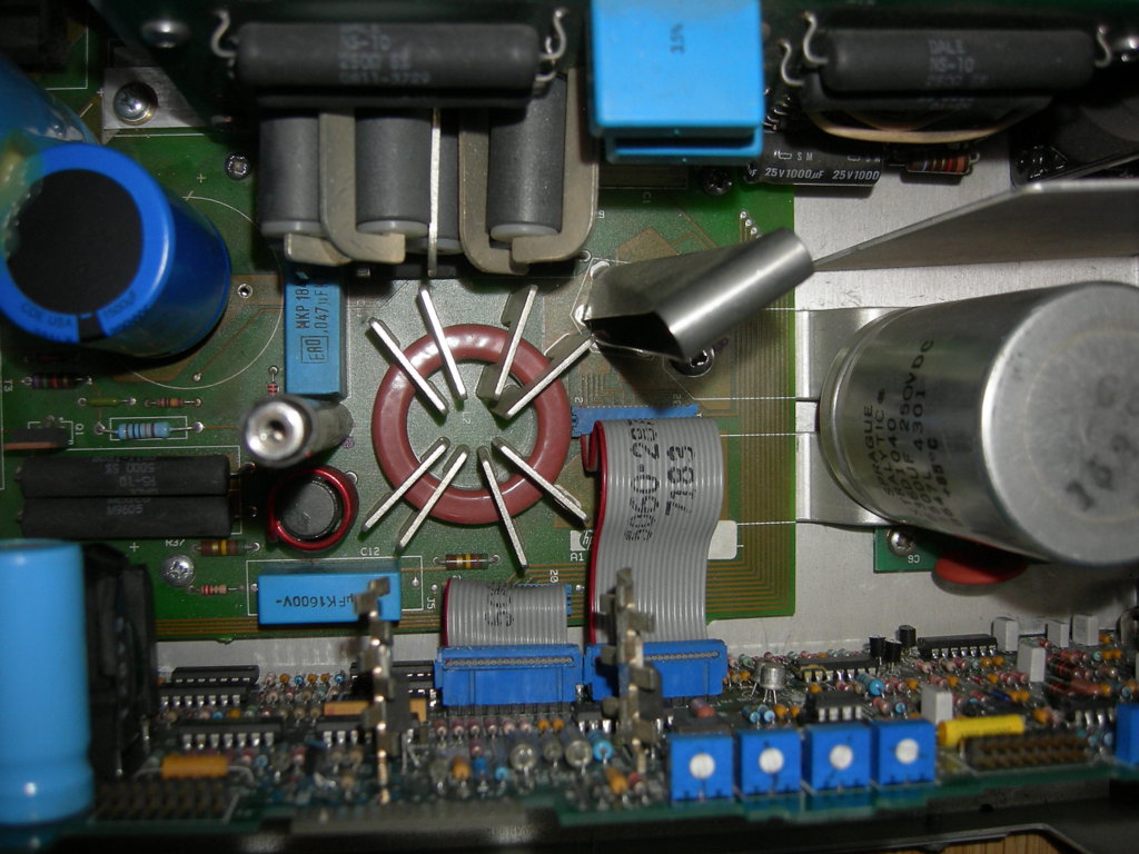
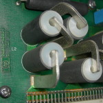
The diode board connects to the system in the same way that the FET board connected to it - via a big DIN connector. The board is nothing but a simple negative rectifier (see the manual for schematic), with some filtering, balancing and something strange. Now, the parts used are either too normal, or very weird - note the inductors:
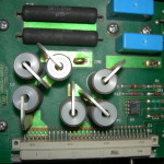
Big ass inductors
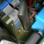
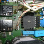
I've never seen this kind of inductors, must be either custom, or very exotic. Either way, they are really big - at 5uH. The diode board also contains a block named "Down programmer" - which as far as I can tell is a system that ensures charge dissipation when you go down with your required voltage. It's a little analog with a power transistor.
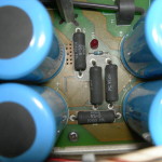
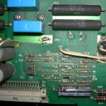
Down programmer
On the heatsink side of the board are just the really power parts -
Power parts on diode board
Only the transistor for the down programmer is visible. The diodes are hidden inside:
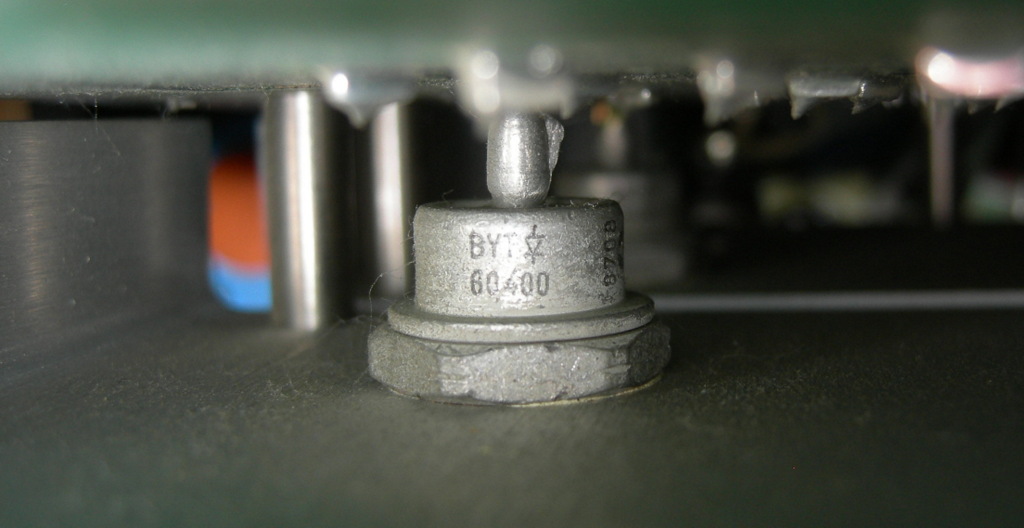
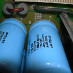
A peek at the diodes
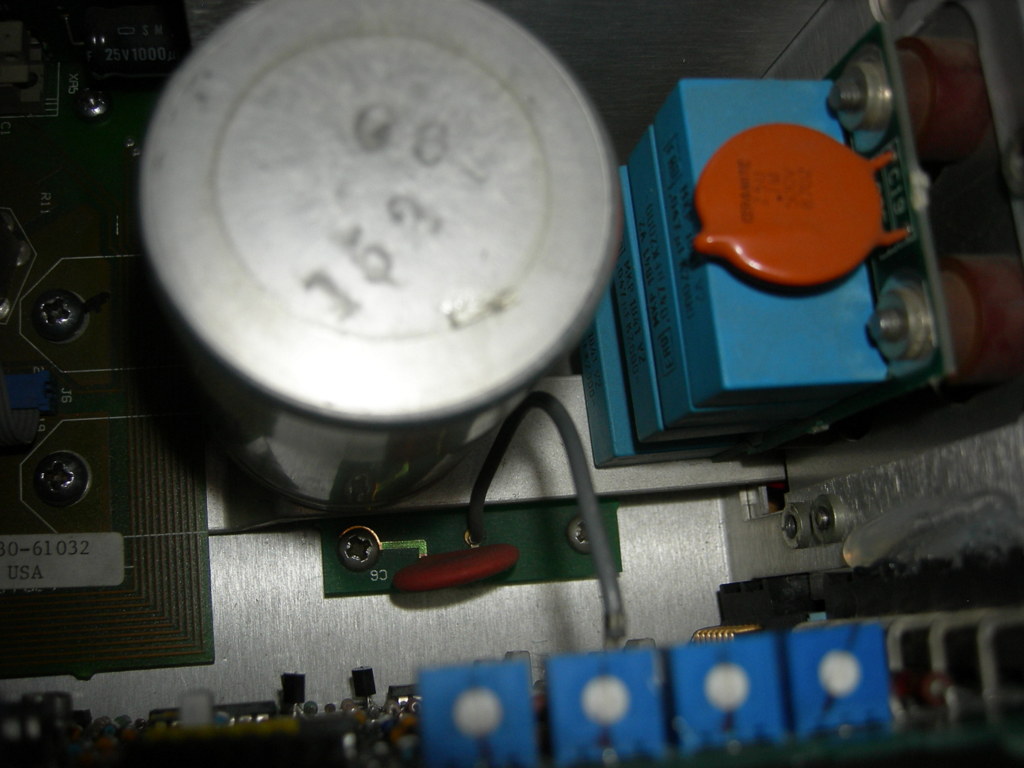
The two diodes are a fast recovery rectifier. And from this board it's back onto the main board to filter, measure and output the voltage.
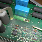
Under the diode board
Now, curiously, the diode board does actually have a connected heatsink, that functions as a connection to the transformer. Why they did this? Must be radiating a lot of EMI. Oh well.
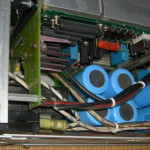
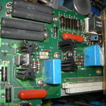
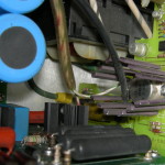
Output state
Now, here's the output from the rectifier board - the bizzare inductor in the middle is a common mode choke. It's pretty much in series with the output. It's a mix of a PCB inductor and soldered in wire blocks. It's really weird. And after that it's on to the main shunt resistor.
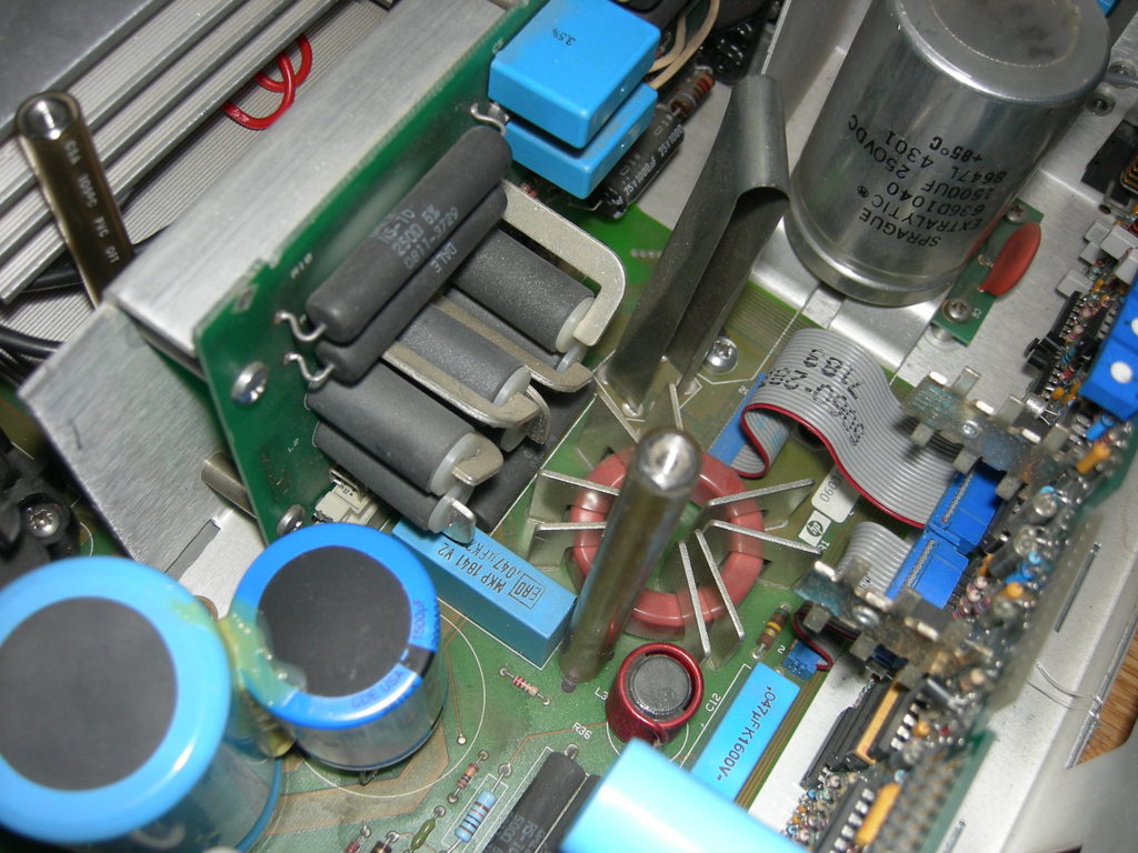
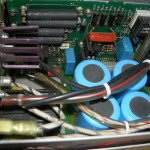
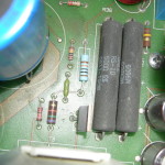
Big ass resistor
It's really a piece of bent metal plate soldered into the board. Its resistance is 1.66 or 3.31 mOhms. Not ohms, but miliohms. I'm sure they had their reasons. This measures the output current and provides part of the feedback for the regulator. After this there's just the output rails and the final filter.
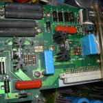
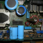
Final filter board, output rails
Well, it's a filter board/assembly. The output rails are led outside, parallel to them a filter capacitive filter is connected. This might not bode well for how fast the current limit kicks in, but I guess that this just isn't that kind of device. There's a big ass main electrolyte cap, then there's a lot of foil caps and finally a ceramic cap.
Final filter board, output rails
And then it's off to the user, to power whatever he needs.
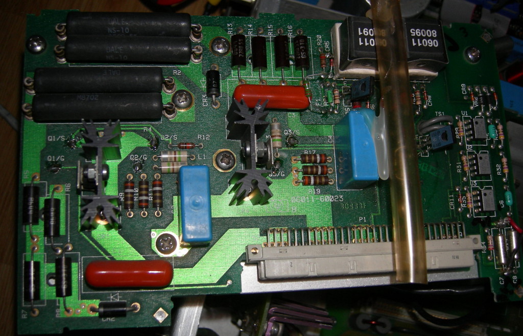
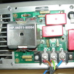
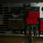
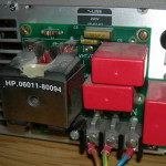
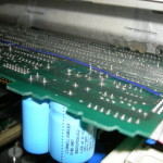
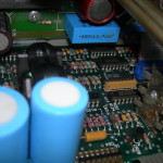
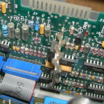
That was the power part. To control this you need a lot of control 🙂 For that we have the control board:
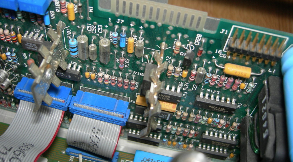
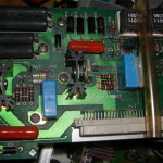
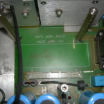
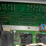
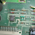
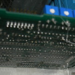
Control board
There's a whole lot of analog stuff going on there, read the manual for details.
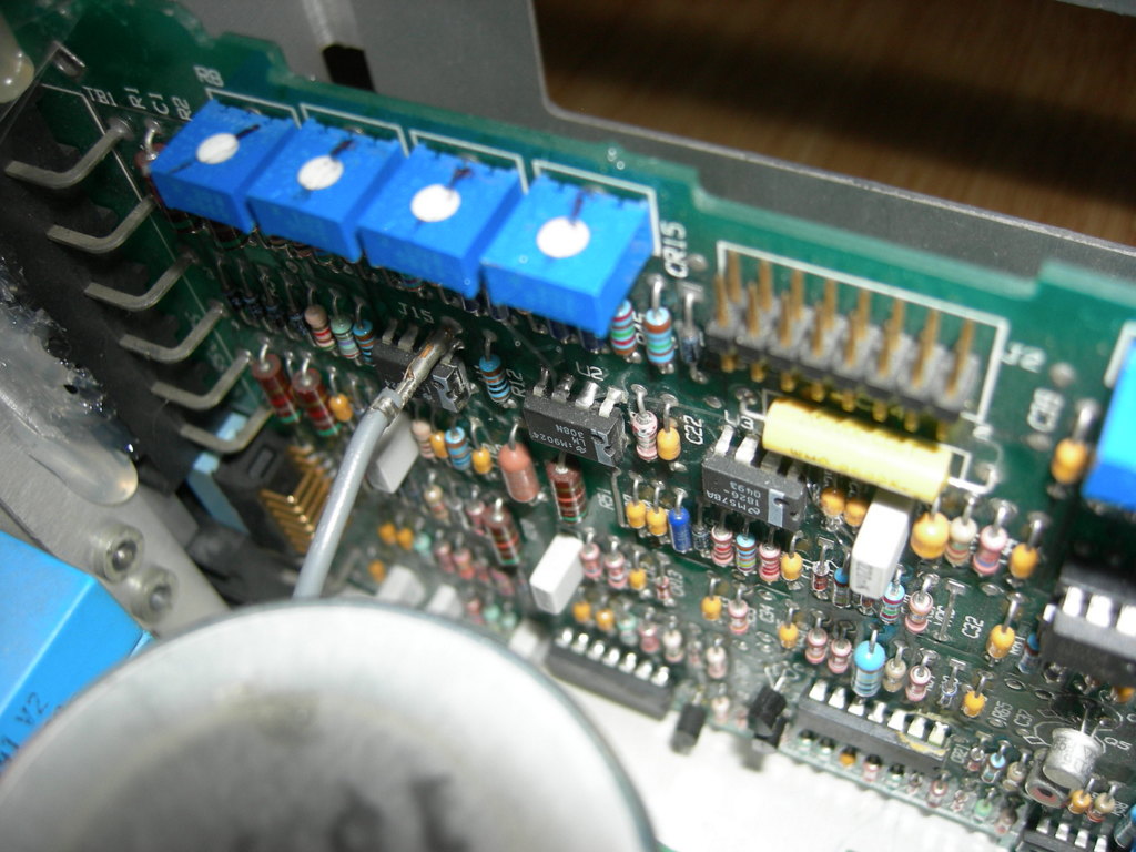
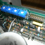
Control board
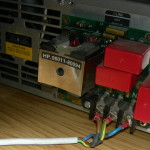
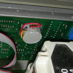
Note that the device has been repaired - several times most likely. Oh well, better than nothing 🙂
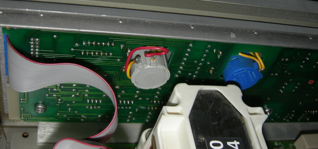
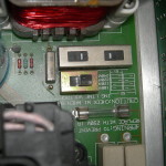
Repaired front panel board
The front panel is mostly just the display and a bit of control stuff. I chose not to remove that. Note that the pots have been changed. A little more butchery?
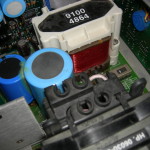
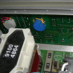
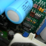
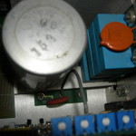
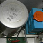
The control part is powered by a separate transformer:
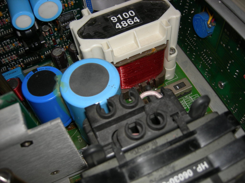
Control power transformer
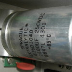
And that about sums it up - the power supply is a scary piece of tech. Repaired, and I do have a few things I don't like in the original design (really big filter cap on the output, should your circuit go short circuit, it'll receive a really big kick from that one before the constant current mode kicks in). Also...:
Fffffffuuuuuuu......
Thanks for reading so far.
David out. Donations will not go amiss 😉
-
- The whole device
-
- The front panel
-
- Side view
-
- The backside
-
- The Fan
-
- Fffffffuuuuuuu……
-
- Output rails
-
- Mains filter
-
- Behold, the Kraken!
-
- Power path
-
- Mains input board connection
-
- FET board top
-
- FET board top – butchery
-
- Well, it works…
-
- FET board connector
-
- Bleeders, filters, the lot…
-
- Mains landing
-
- Hey there, big fella…
-
- Control power transformer
-
- Control power transformer
-
- Diode board top
-
- Big ass inductors
-
- Down programmer
-
- A peek at the diodes
-
- Under the diode board
-
- Power parts on diode board
-
- Behind the transformer
-
- Output state
-
- Big ass resistor
-
- Control board
-
- Control board
-
- Final filter board, output rails
-
- Final filter board, output rails
-
- Repaired front panel board


7 Responses to HP 6010A Teardown