While on a buying frenzy at a local radioamatuer gettogether (Holice 2014) I saw an interesting looking PCB - apparently taken from some kind of older HP system, it had some very nice oscillators (500, 525, 100, 126 MHz), some nice SMA and SMB (note: I've mislabeled them as SMC) connectors and a few other interesting miscellany items. Seeing as it was being sold for the equivalent of ~6 EUR I indulged myself and bought it.
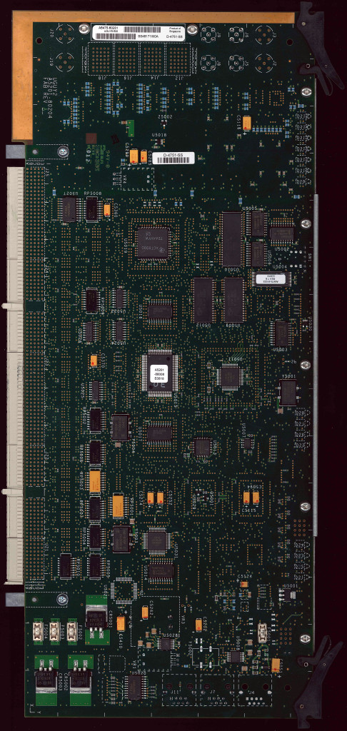
Later on I did some digging, it turned out to be a utilities board for the HP 9000 series Superdome, a PA-8xxx based server system that packed some serious power for its era. It's an impressing piece of tech, seemed a shame to just rescue the oscillators from it and discard the rest, so, I've scanned it for the good people of the internet to see.
There's a bit of guesswork I did as well as to the function of the board and its various blocks - since no datasheet exists specifically for that board I did a few guesses based on what I saw.
Functions
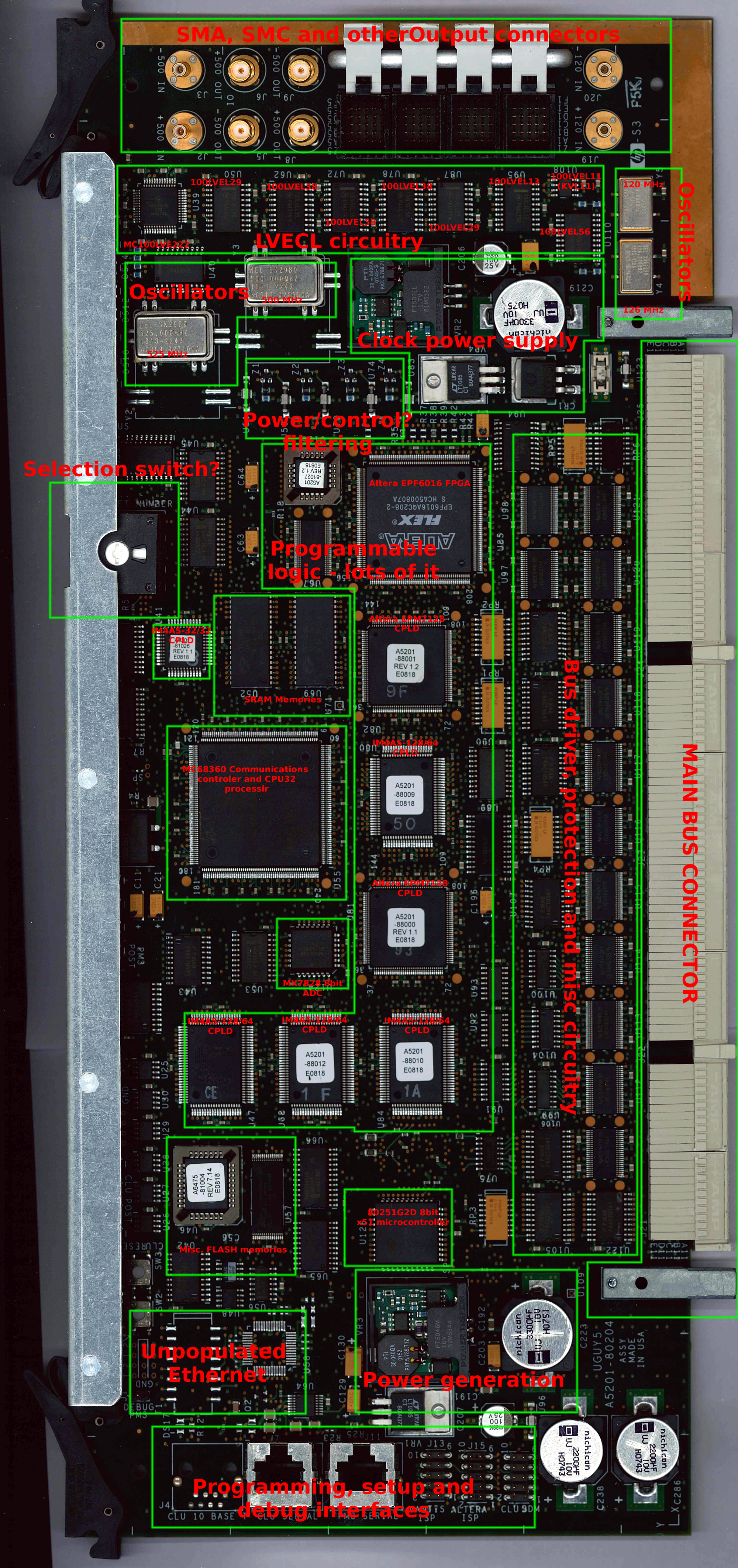
Part of the main function of the board seems to be clock generation and distribution. This is indicated by both the coax connectors leading from the board as well as into the board. There's a few LVECL logic (Low Voltage Emitter Coupled Logic) devices, 500 MHz, 525 MHz, 126 MHz and 100 MHz (and some misc) crystal oscillators with ECL outputs (NEL made SJA2920 and SK29B9 devices). There are also connectors labeled RBP, LBP, IO and IO - which I assume mean Right BackPlane, Left BackPlane, IO and IO - so I guess it's a clock source for these areas. Although it might also be a clock monitor, seeing as there are 500 MHz inputs (and outputs as well) and 120MHz inputs only. But I find that unlikely, seeing as there is a 1:15 clock distributor IC there as well. I'd love to know more.
The other functions should probably be categorized under miscellany - a bit of this and a bit of that. Some debugging? Some low level control? Power monitoring? I honestly can't say - the logic on the board does not indicate anything specific - it's all general purpose logic, bus drivers, a fair amount of programmable logic, but nothing to indicate any specific function - all of that hardware is very general purpose. You can plug in an RS232 connections in at least two places - probably console like ports. These are driven by MAX3221 devices.
There are some things that were not populated - without too much guessing I'd say that the board can support an 10 Base T Ethernet connection, but that area is unpopulated. The 500ish MHz crystal oscillators have a footprint that seems to indicate that other types can be used as well.
The build quality, what to observe, the design
Well, the build quality is superb as far as I can tell.
The board is quite thick (2.4mm) and without a doubt has at least 6 layes (top, internal routing 1,2, power planes, bottom), but it's reasonably certain that there are at least 10 layers, probably more.
All of the parts are SMD with the exception of the connectors and two switched voltage regulator modules - even the pretty massive 3300uF/10V capacitors are SMD. This is a good way to lower assembly costs and improve yield - you only stick your pretested board into the pick and place machine and out comes a fully assembled board. There are techniques to solder non-SMD components with reflow soldering, so you get all your soldering done in one step.
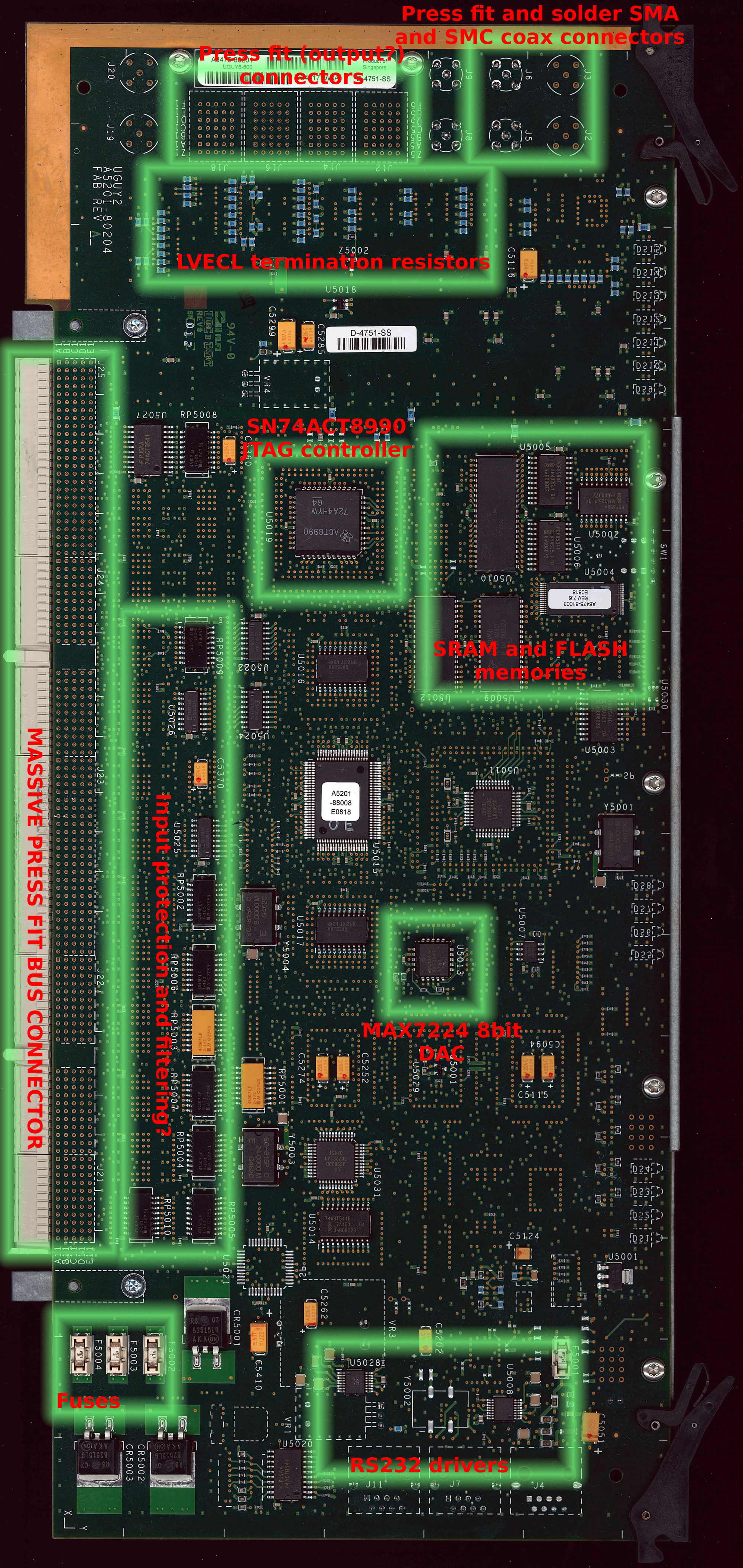
This technique is not applicable however to some of the connectors - the big, million connection scary connector that connects to the system bus for one, and the many many pinned monsters as well. So, in comes press fit technology - basically you make a smaller hole, and press the part inside. Obviously, you have to have a part that supports this, but it's a popular, solder-free technique for this kind of things. On this particular board it was used on the main bus entry connector, the clock distribution (?) connectors, and the coax SMB connectors.
Routing
Pretty much all of the signal and power routing is in the inner layers. Probably done to maintain signal integrity and limit noise radiation/pickup - the signals lines are most likely squished between plane layers. There are a few lines here and there, but they disappear very quickly into a via or a component.
The power distribution is done most likely through power planes as is the norm in this kind of system (and a very reasonable norm it is).
Power
The board contains four power source devices - PT5031L, PT5046M, 2x LT1085 and one device that could be a regulator. There does not seem to be enough power to power the main logic - the LT1085s source +3.3V (based on the resistive divider next to them), but 2x3A for all of the logic on that board seems quite small - these kinds of devices can be quite power hungry. On the other hand, who knows, the main bulk of the logic can be running quite slowly. The switched voltage regulator modules are for different voltages - +10V, -1.7V (probably some ECL thing).
I would have expected a heftier point of load regulator. I don't think that there's a global power supply somewhere behind the bus - a summed up current of all 3.3V devices on a big system might be scary.
Another thing to observe is the decoupling - all done properly, just as it should be. Every IC has a decoupling cap very close to it, with a via leading down into a power plane on both sides. Nicely done.
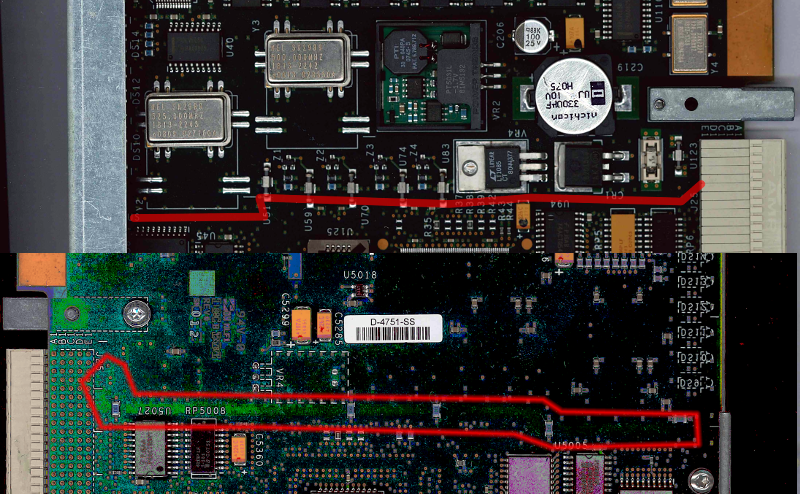
There's a power plane split as well - the ECL part of the board connects to the rest of the board through series filters - see:
I've had to highlight it - the scan of the board barely shows it, but when you look at it against a light source, the gap is clearly visible.
Each of the series filters ( U51 for instance) is an SMD series low pass filter - basically a ferrite bead with a capacitor in the middle. This way one part of the board does not send interference to the other. Whether these are power only signals or there are control signals as well I can't say 🙁 My guess is power only. There are also some connections on the bottom side done through a series connected 10 ohm resistor. These might be the control signals. I honestly don't know. Doesn't seem to be a lot of them though.
Other
Well, in the misc part of the text I shall include what is probably the main functionality of the board - the bus communication logic and overall board intelligence.
The MC68360 communication device and processor serves as the brain of the board. This device is surrounded by several programmable logic devices from Altera and Lattice, a few memories and miscellany support logic and ICs. The programmable logic probably handles part of the bus communication and talks to the bus drivers circuitry. The bus driver circuitry are mostly bus driver ICs, like the 74LVCH162244A and similar.
One interesting thing on the bottom of the board is a JTAG controller SN74ACT8990 - it's a JTAG master device, which means that it can JTAG its way into whatever chain is connected to it. Neet!
And there's an ATMEL 80251 controller on the board. Probably a VERY low level controller for something.
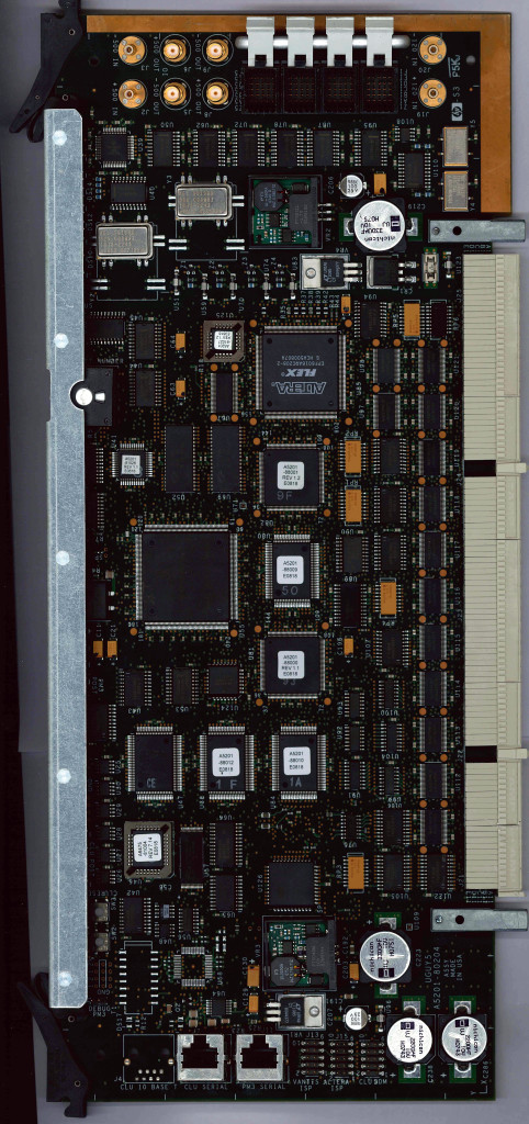
And, that's about it - all in all a nice board, well worth the 6 EUR spent. Under the article you should see the actual photos and a highlight of the parts in question. Click on the images for a full resolution image.
To view the actual scans in full resolution, you should click on them.


Pingback: Under the Hood – What Does this Board Do? | Hackaday