
This is the second part of the teardown of the HP 3455A digital multimeter. It will deal with the logic part of the device. You can read the first part of the teardown HERE. And the last part, for the analog part, where all of the magic happens HERE.
Once you open this up, you will be greeted by this image:
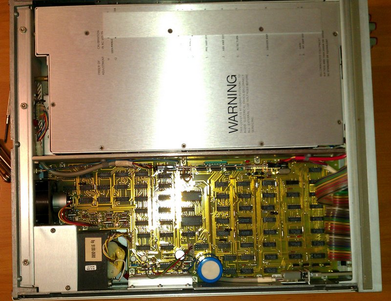
The device with the cover taken of
On the top part you can see the analog part - that's the one that's fully shielded. These guys meant business. On the bottom part it's the digital part where all (or some at least) the calculations are done. And the display is controlled. And the user interface. And the GPIB-ish bus. And the power supply.
The power supply is where it all starts. You can see it here:
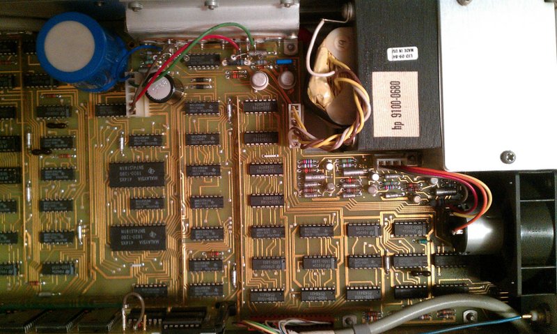
Another shot of the power supply
It's nothing special really - just a transformer and a linear power supply that gets the makes the required voltages. There's a pretty big heatsink. Also, there's a fan for the digital logic part - it generates a lot of heat apparently.
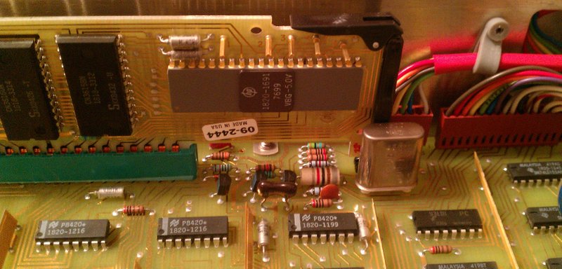
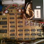
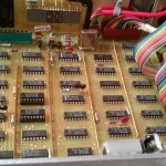
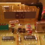
The digital part is pretty boring really - it's pretty standard (albeit well designed and done) for this era of technology. A simple processor (one that uses an external ALU, memory and other features) controls the whole system through a (fairly) simple program. Here's the processor board:
The CPU module itself
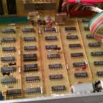
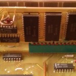
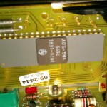
Yes, the logic board has a processor board, for some reason. And the processor, well, it's a "nanoprocessor" - from what I've found on the internets, it's a proprietary custom HP device. Because GO TO HELL STANDARD REPLACEABLE STUFF, THAT'S WHY! The small board contains ROM memories:
The CPU module itself - Memory (most likely)
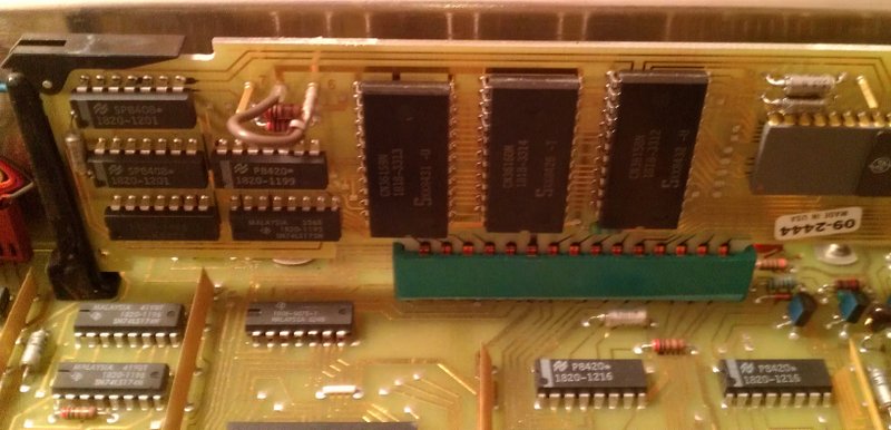
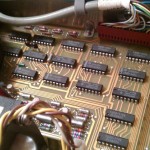
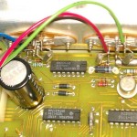
And the craziest jumper I've ever seen. The processor itself is a simple thing apparently - it doesn't even have an ALU of its own (as there is one placed on the board below). You don't get much simpler than that. Here's a shot of the ALU... and shockingly even more logic!
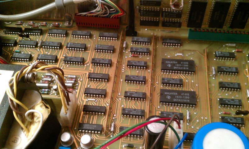
More logic
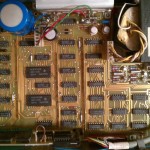
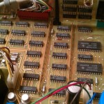
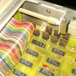
The board also handles the display driver and muxing. So, here are the drivers and the connection:

Display drivers
One small detail that I noticed: HP uses its own part numbers and it doesn't matter as to whom they are from originally. Note the various brands of ICs there - AMD, Ti, there's a Motorola somewhere as well, and all of them are either completely renumbered, or have the HP part number added as well.
Another fun thing I'm not used to in this era is the power distribution bar - note the yellow little bars on the PCB. They are the distributor for the power.
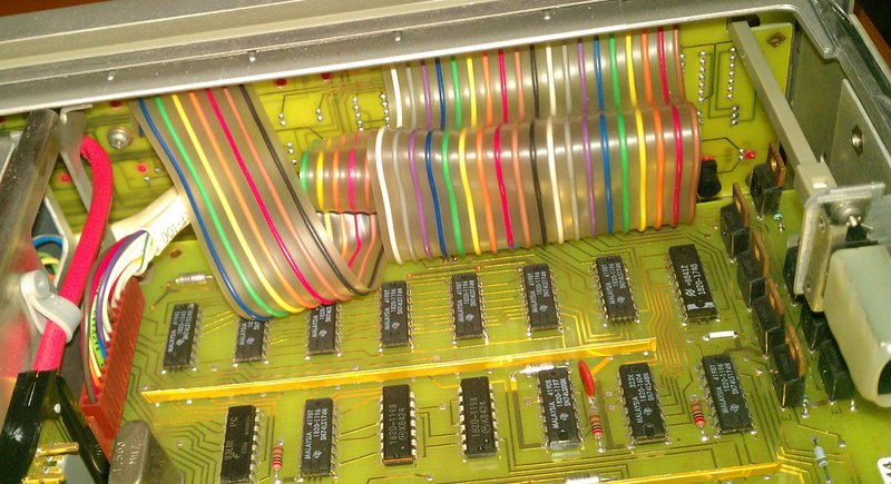
Display and keyboard connection and control
Those who were paying attention will note that I have not shown the display and keyboard PCB. There's a simple reason - it would require too much disassembly of the whole system and what exactly can we find? Buttons and LEDs? Interesting, tempting even, but not that much. Sorry.
And here's the gallery - a few snaps of these were not in the original text. And stay tuned for the next part, where we shall take a peek into the analog part, which is a piece of art! Enjoy!
-
- The device with the cover taken of
-
- The power supply region of the logic board
-
- Another shot of the power supply
-
- Another shot of the power supply
-
- Connection to another part of the device
-
- Main clock source and more logic
-
- Another shot of the crystal
-
- More logic
-
- The CPU module itself
-
- The CPU module itself – Memory (most likely)
-
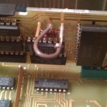
- The HP jumper, also known as WTF?
-
- Power supply detail
-

- Fan detail
-
- Display and keyboard connection and control
-
- Display drivers
-
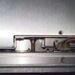
- The bus interface

4 Responses to HP3455A teardown - part 2 - The Logic! and the Display